( Nanoelectronics) Principles of construction and classification of NEMSs (PhD in Micro _ Nanoelectronics)
Researcher and author: Dr. ( Afshin Rashid)
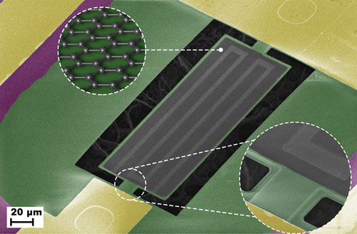
tip; NEMS through nanoelectronics in systems that are classified for defense, pharmaceutical, medical, electronic and telecommunication applications, etc. NEMS current that includes acceleration gauges are, chip display projection, the drone sensors, optical switches, Microvalve and multi-functional biosensors and micro-chips used in nano-volumes are produced.
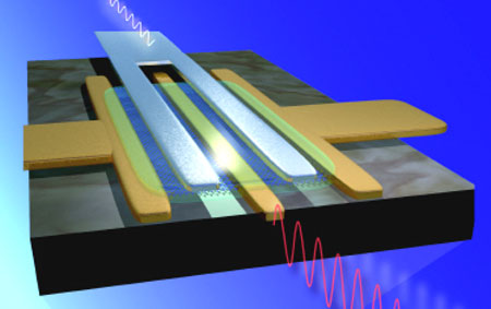
NEMSs are integrated into moving microstructures (with electromechanical components ), sensors, actuators, radiation energy devices, and microelectronics. These N EMSs can be built for use in various microstructure technologies such as micromachines . Basic technology in the construction of NEMS , CMOS and biCOMS (for the construction of ICs) and micro-machines (for the production of motion and radiation and energy radiation to devices and structures ). This is one of the main objectives of microelectronic devices and structures with make-up machines, electro-mechanical, not complex to NEMS are integrated and high-efficiencyکردن. To ensure high performance, workability, reliability and buildability, bulk manufacturing processes based on CMOS are well developed and should be modified and enhanced.
Micro-up (Micromachining (the trunk (BULK, (plus Fnavy of the upper case ( , (LIGA-like and LIGA) or) high - aspect ratio most developed methods of construction. Silicon material below the initial layer is the industry microelectronics A number of crystal molds ( solid 300 mm diameter and 100 mm long) are crystallized from very high purity silicon and cut to the desired thickness and then polished by mechanical and chemical polishing technologies . electromagnetic and mechanical direction and crystallized the crystals and impurities predicted it. depending on the layer of silicon CMOS processes and biCMOS for ICs are used to produce and processes are classified as: n-well-n, well-p (well-p) or well-twin. The main steps are: diffusion (oxidation ). , (Polysilicon, photolithography), gate formations Masking, etching, metallization, wire bonding, etc.
Conclusion :
NEMS through nanoelectronics in systems that are classified for defense, pharmaceutical, medical, electronic and telecommunication applications, etc. NEMS current that includes acceleration gauges are, chip display projection, the drone sensors, optical switches, Microvalve and multi-functional biosensors and micro-chips used in nano-volumes are produced.
Researcher and author: Dr. ( Afshin Rashid)
PhD in Nano-Microelectronics


