_ Nanoelectronics and Plasmonic Particles Department
Nanoelectronics and Nanoplasmon Polaritons (Surface Plasmon Polariton)
Researcher and Author: Dr. ( Afshin Rashid)
Note: Surface Plasmon Polariton is the non-diffusive excitation of conduction band electrons in metallic nanostructures to which an electromagnetic field has been coupled. Plasmonic waves arise from a conducting nanoparticle whose dimensions are below the wavelength of the excitation electromagnetic field using the scattering problem.
The interaction of a particle of size d with electromagnetic waves of excitation wavelength λ can be investigated in various analytical, semi-analytical and numerical methods. Of course, in these analyses, the assumption is always taken into account that d≪λ, i.e. the particle dimensions are much smaller than the wavelength. The phase of the harmonic oscillation of the electromagnetic field in the particle volume is assumed to be constant.
The following conditions affect the excitation of localized surface plasmons and their characteristics:
_Electronic properties of nanoparticles
_ Dimensions and shape of nanoparticles
_ Thermal properties of nanoparticles
_ Dielectric surrounding the nanoparticle
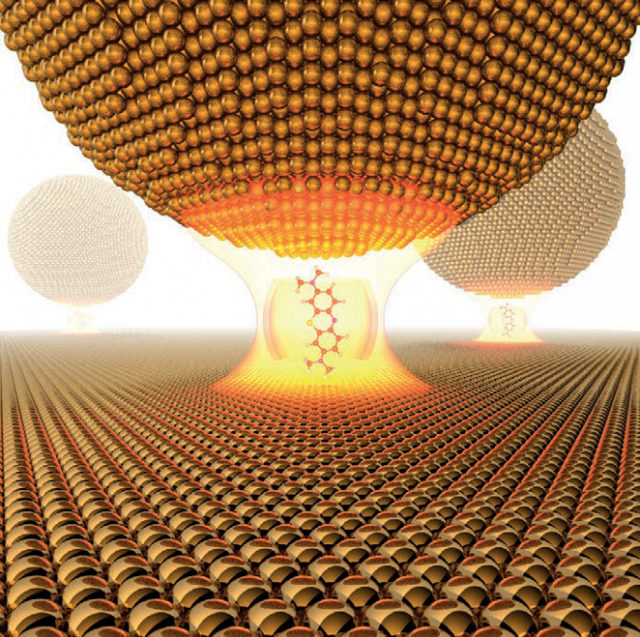
It is important to note that the intensity of the electromagnetic field (specifically the electric field) decreases exponentially with distance from the surface of the metal nanoparticle. In this created nanovolume, the electromagnetic field is locally compressed and enhanced. Slight changes in the dielectric surrounding the nanovolume affect the resonance of surface plasmons, so that these changes are reflected in the amount of scattered light, absorbed light, or a change in its wavelength. These changes can be measured using optical characteristics. The oscillation of surface electrons and the electric field around them is reflected in the resonance of local surface plasmons. The name polariton was used for quasiparticles that were half matter and half photon, which is the coupled state between a photon of the primary excitation beam and the conduction electrons of the metal, and the term plasmon polariton is used to express the coupling between a photon and a plasmon.
Surface Plasmon Polariton is the non-diffusive excitation of conduction band electrons in metallic nanostructures to which an electromagnetic field has been coupled. Plasmonic waves arise from a conducting nanoparticle whose dimensions are below the wavelength of the electromagnetic field of the excitation beam using the scattering problem.
Researcher and Author: Dr. ( Afshin Rashid)
Specialized PhD in Nano-Microelectronics


