_ بخش نانو الکترونیک و ذرات پلاسمونی
کاربرد علم پلاسمونیک در فشرده سازی مدارات و اُلگوی اَفزاره های نانو الکترونیک
پژوهشگر و نویسنده: دکتر ( افشین رشید)
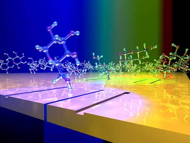
نکته: با رویکرد تکنولوژی به سمت تجمع مدارات الکترونیک نوری، مشکلات ساخت و پدیده هایی که به جلوگیری از فشرده سازی بیشتر ساختار کمک می کرد، باعث شد تا استفاده از ساختارهای پلاسمونیک و امواج پلاسمونیک مورد بررسی و استفاده قرار بگیرد. این نانو ساختار ها متشکل از فلز و دی الکتریک می باشد که ابعاد آنها زیر طول موج تحریکی ( طول موج پرتویی که باعث تحریک امواج پلاسمونیک می شود) قرار دارد.
پلاسمونیک بر اساس فرآیند برهم کنش بین امواج الکترومغناطیسی و الکترون های رسانش در فلزات با ابعاد نانو بیان شده است.به صورت تحلیلی دلیل افت سریع انرژی الکترون ها در عبور از فلزات میباشد و نتیجه گرفت این انرژی صرف حرکت تجمعی و نوسان گونه الکترون های آزاد فلز می شود و آن را پلاسمون نامید. دلیل این نام گذاری شباهت این نوسانات الکترون ها با نوسان های ذرات محیط پلاسما بود. به اصطلاح عبارت پلاریتون را برای نوسان الکترون های مقید فلز در حالت جفت شدگی با فونون های پرتو فرودی به کار میرود. نام پلاریتون برای شبه ذراتی که نیم ماده و نیم فوتون بودند، بکار گرفته شد که حالت تزویج شده بین یک فوتون پرتو تحریک کننده ابتدایی و الکترون های رسانش فلز است و اصطلاح پلاسمون پلاریتون (Plasmon Polariton) برای بیان علت تزویج شده بین یک فوتون و یک پلاسمون است.
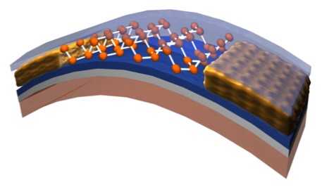
تقسیم بندی این علم نوپا به دو حوزه پلاسمون های سطحی موضعی و پلاسمون پلاریتون های سطحی هر یک به طور اجمالی معرفی می شود. در پلاسمون های سطحی موضعی اساس برهم کنش ها نانو ذرات می باشد که به بررسی خواص آنها در تحریک این مد از امواج پلاسمونیک پرداخته شده است. در پلاسمون پلاریتون های سطحی با معرفی بنیاد کاری آنها فرمول بندی میدانی آن و چگونگی گذشتن از حد پراش توسط این ساختار ها وجود دارد.نانو ساختار ها ، هم از جهت سنتز و تولید، و هم از جهت خواص و کاربرد ها تفاوت های اساسی با هم دارند. به طور کلی خواص الکتریکی، نوری، مغناطیسی، سطحی و غیره این سه ساختار با یکدیگر تفاوت های اساسی دارند و بالطبع کاربرد هایشان نیز متفاوت است.از نانو ساختار های یک بعدی می توان برای اتصالات الکترونیکی استفاده کرد درحالی که برای نانو مواد صفر بعدی و دو بعدی چنین کاربردی وجود ندارد.پایه اصلی نانو تکنولوژی بر استفاده از مواد است. هر ماده ای در فضا دارای سه بعد طول، عرض و ارتفاع است. اگر در ماده ای حداقل یکی از این سه بعد در محدوده نانو متری باشد به آن یک ماده، یک نانو ساختار گویند.

نتیجه گیری :
با رویکرد تکنولوژی به سمت تجمع مدارات الکترونیک نوری، مشکلات ساخت و پدیده هایی که به جلوگیری از فشرده سازی بیشتر ساختار کمک می کرد، باعث شد تا استفاده از ساختارهای پلاسمونیک و امواج پلاسمونیک مورد بررسی و استفاده قرار بگیرد. این نانو ساختار ها متشکل از فلز و دی الکتریک می باشد که ابعاد آنها زیر طول موج تحریکی ( طول موج پرتویی که باعث تحریک امواج پلاسمونیک می شود) قرار دارد.
پژوهشگر و نویسنده: دکتر ( افشین رشید)
دکترایِ تخصصی نانو _ میکرو الکترونیک

