

_ بخش (نانو و میکرو اِلکترومکانیکال MEMS)
(نانو و میکرو اِلکترومکانیکال MEMS) در اَدوات نانو اُپتیکـی (xAs-AlxGa1) در (حالت 45.0<x)
پژوهشگر و نویسنده: دکتر ( افشین رشید)
نکته: سیستم های (نانو و میکرو اِلکترومکانیکال MEMS) در ادوات نانو اپتیکـی (xAs-AlxGa1) را در (حالت 45.0<x) به همراه تغییرات فاصله لبه نوار ظرفیت با لبه نوار هدایت با تغییرx در سه راستای مختلف انتشار موج پیدا میکند.
به سبب نبود عایق مناسب برای به کارگیری در گیت ترانزیستورها و نیز گرانی عناصر و فرایند لایه نشانی نیمه هادی های مرکب ،سیلیکون و نهایتاً آلیاژ سیلیکون ـ ژرمانیوم همچنان به عنوان نیمه هادی اصلی مورد استفاده باقی مانده است.لازم به ذکر است سیستم های (نانو و میکرو اِلکترومکانیکال MEMS) ، که به سهولت قابل لایه نشانی با خلوص بالا است، عایق بسیار مناسبی برای این منظور است. امروزه در مدار های مجتمع با طول کانال زیر 50nm از اکسید های جایگزین با ضریب دی_الکتریک بالاتر مانند اکسید زیرکونیوم ZrO2 و اکسید هافنیوم میگیرند بهره HfO2 در آلیاژهای سه تـایی از زوج مواد مرکب عناصر میتوان با تغییر نسبـت دو عنـصر موجـود خصوصیات متفـاوتی بـرای نیمه هـادی به دسـت آورد. به عنوان مثـال، در xAs-AlxGa1 و xN-InxGa1 تغییـر x به تغییـر گاف انـرژی و بسیـاری از خصوصیـات این مواد مرکـب نیمـه هـادی منجر انـرژی نوار ساختـار میشـود.

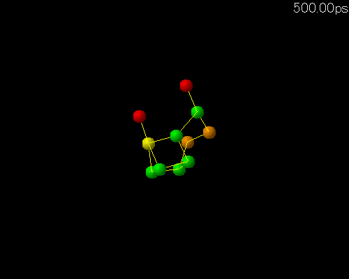
در ساختار سیستم های (نانو و میکرو اِلکترومکانیکال MEMS) یکی از مهمترین خواص نانو ذرات فلزی خاصیت الکترونیکی است. نانو ذرات فلزی یک نیمه رسانا با شکاف باند صفر و رسانایی الکتریکی بالا است. همان طور که میدانیم هر اتم کربن دارای 1 الکترون است که در پیوندهای شیمیایی شرکت میکنند، اما در گرافن هر اتم کربن در یک فضای دو بعدی به 9 اتم کربن دیگر متصل است. تک اتم های باقی مانده، ایجاد اوربیتال پای در بالا و پایین صفحه گرافن کرده و این اوربیتال ها ایجاد پیوند های دو گانه کربن-کربن میکنند. خاصیت الکترونیکی در سیستم های (نانو و میکرو اِلکترومکانیکال MEMS) توسط (اوربیتال پیوندی) و(ضد پیوندی) پیوند های دوگانه به گرافن تحمیل میشود. گرافن تحرک الکترونی بسیار بالایی را در دمای محیط نشان میدهد.

در ساختار سیستم های (نانو و میکرو اِلکترومکانیکال MEMS) استحکام اُپتیکی نانو ذرات فلزی 22 مقاومت شکستن m N 12 و ضریب یانگ آن Tpa 4 میباشد. علی رغم سختی و استحکام بالا، بسیار سبک بوده و چگالی آن در حد (ml/mg 77/1) میباشد. خواص (اُپتیکی) غشا مونو لایه ای نانو ذرات فلزی با تکنیک AFM اندازه گیری میشود.

نتیجه گیری :
سیستم های (نانو و میکرو اِلکترومکانیکال MEMS) در ادوات نانو اپتیکـی (xAs-AlxGa1) را در (حالت 45.0<x) به همراه تغییرات فاصله لبه نوار ظرفیت با لبه نوار هدایت با تغییرx در سه راستای مختلف انتشار موج پیدا میکند.
پژوهشگر و نویسنده: دکتر ( افشین رشید)
دکترایِ تخصصی نانو _ میکرو الکترونیک