

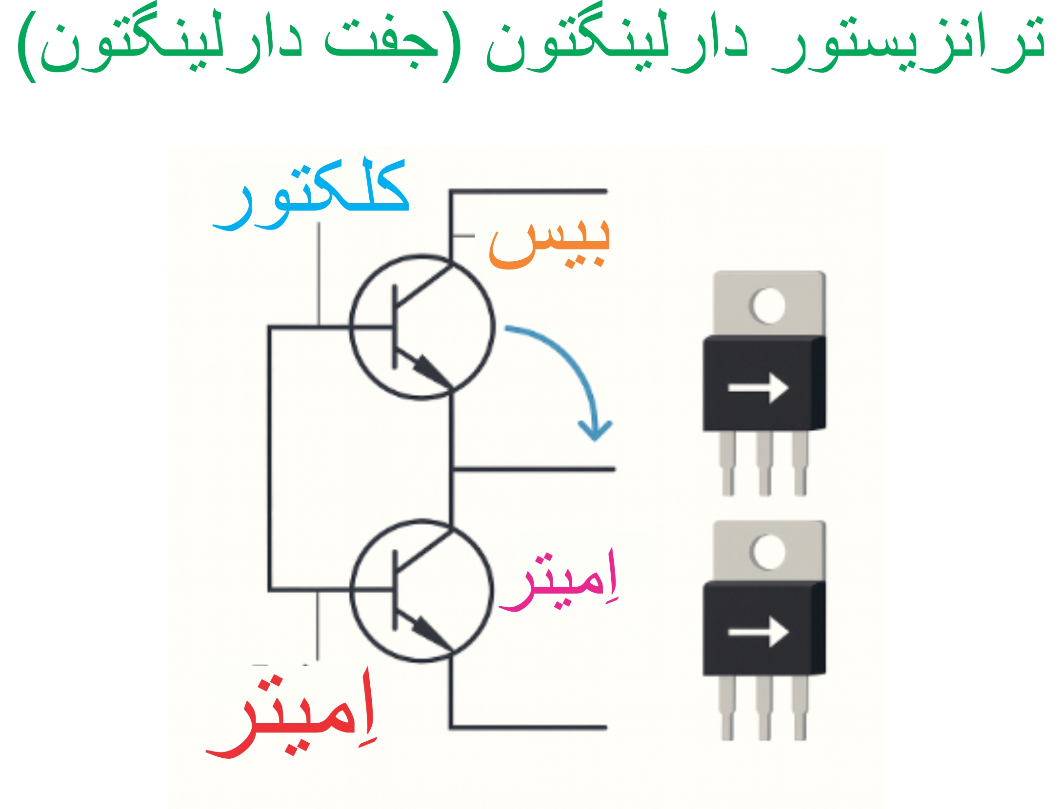
Section _ Understanding (Darlington transistor ) or Darlington pair
Investigation (cut-off logic) in Darlington transistor (Darlington pair)
Researcher and author: Dr. ( Afshin Rashid)

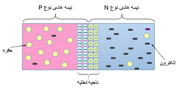
In the structure and internal structure of the Darlington transistor, in this region, the applied input voltage is not enough to turn on the device and the applied voltage has not reached the excitation voltage. If a positive voltage is applied to the emitter, the pn junction remains in reverse bias until the input voltage is less than a certain value. Under this condition, holes are injected from the p-type material into the n-type rod. These holes are repelled by the positive electrons.

The two terminal connections of the N region are called the ( base) and the P-type semiconductor connection is called the emitter. The ohmic resistance of the N-type semiconductor is high and is about 4 to 10 kilohms . The Darlington transistor can be represented as an equivalent circuit. If we keep the emitter (E) terminal open and establish a potential difference across the two ends of the N-type semiconductor, it is called the Darlington division factor of the Darlington transistor , the value of which is specified by the manufacturer.
_ife5.gif)
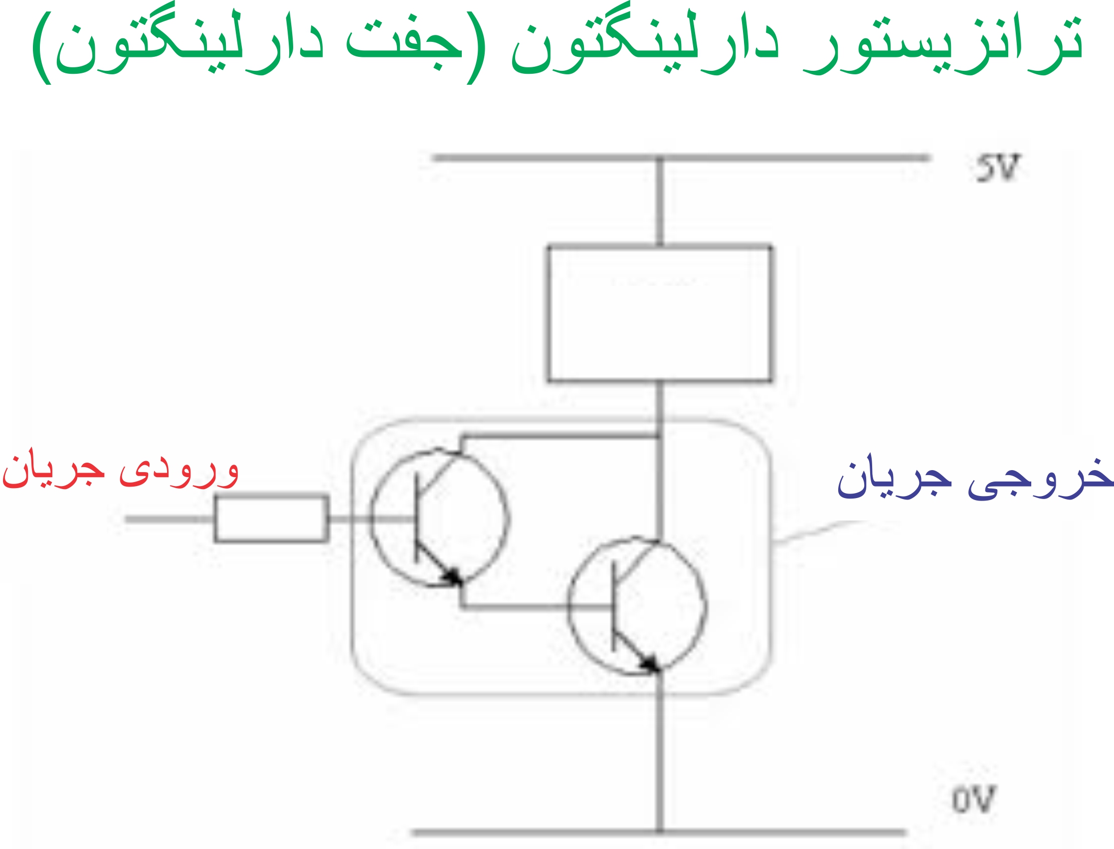
The Darlington transistor is “on”. At this point, the emitter impedance is reduced to B1 as the emitter goes into low impedance saturation and emitter current flows through R1 . Since the ohmic value of resistor R1 is very low, the capacitor is discharged rapidly through the Darlington transistor and a rapidly rising voltage pulse appears across R1 . Also, since the capacitor is discharged faster through the Darlington transistor than it is charged through resistor R3 , the discharge time is much less than the charge time because the capacitor is discharged through the low resistance Darlington transistor . When the voltage across the capacitor drops below the pn junction holding point ( V OFF ), the Darlington transistor turns off and no current flows to the emitter junction, so the capacitor is recharged through resistor R3 and this charging and discharging process between V ON and V OFF is repeated continuously until the supply voltage V is applied.
Researcher and author: Dr. ( Afshin Rashid)
Specialized PhD in Nano-Microelectronics