

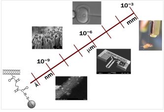
_ Department (Nano and Micro Electromechanical MEMS )
Investigation of the ( nano- electric and mechanical) process in nano-electronic and nano-electro-optical devices
Researcher and author: Dr. ( Afshin Rashid)
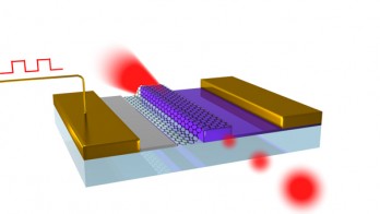
Note: Different MEMS and NEMS must be designed according to the specifications of the needs, goals, and applications. Electromechanical and optomechanical MEMS and NEMS have been developed. Typically, optical systems are faster, simpler, more efficient, more reliable, and more durable than electromechanical systems.
Although optical systems are designed for different applications (such as communications, computing, wireless keying, etc.), they have different configurations, making it very difficult to make a comparative comparison between them. For example, optical systems cannot be used as actuators. The application requirements must be considered, and electromagnetic coupling, temperature, vibration, or radiation can be factors used to design better. As another example, let's look at nano- and micro-scale actuators. The size of the actuator depends on the amount of force or torque that can be generated, which is a function of the material used and its size (volume). In fact, the size is determined by the required force and torque and its type . This is very important when electromagnetic MEMS, microstructures or microtransistors, which are integrated with ICs used in micro-electronic devices, are controlled. Thus, microstructures and microtransistors, electronic devices and ICs must be integrated. Direct chip connection technology has advanced greatly. In particular, chip-flip assemblies of MEMS have been replaced by wire-band to connect ICs with micro-nano-scale actuators and sensors. The use of chip-flip technology allows for the removal of inductors, capacitors and parasitic resistors.

This leads to refinement of the device specifications. Further, chip-flip integration offers advantages in implementing advanced flexible packages, reliability improvements, and weight and size reductions, etc. Chip-flip integrated, microtransistors can be mounted with the bumps facing down on the layers mounted on electromechanical devices and connected to the IC base. Large-scale integrated MEMS (a chip that can be mass-produced and is low-cost, which is used in COMS).

Conclusion:
Researcher and author: Dr. ( Afshin Rashid)
Specialized PhD in Nano-Microelectronics