Department of systems (nano and microelectric and mechanical MEMS )
Stage 1 (Crystallization of silicon dioxide (grow silicon dioxide).
Researcher and author: Dr. ( Afshin Rashid)
(Silicon dioxide is crystallized by a thermal method on a silicon base. For example, crystallization can be done in a space full of water vapor at a temperature of 1000 degrees Celsius and for one hour. Silicon surfaces with a layer with a diameter of 5 0 to 1 micron are covered by silicon dioxide (the thermal oxide thickness is limited to a few microns as a result of the diffusion of water vapor along the silicon oxide). Silicon dioxide can be deposited without changing the surface of the layer, but this process is so slow. which minimizes the pressure of the thin membrane.Silicon nitride may also be deposited and its thickness is limited to 4 to 5 micrometers.
Nano-silicon particles are also available in ultra-high purity and high purity carbon and dispersed coatings. They are also available as dispersions via nanofluids. Nanofluids are generally defined as nanoparticles suspended in solution using either surfactant or surface charge technology.
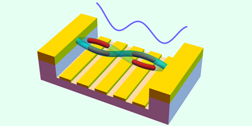
Silicon nanoparticles (Si NPs) have received attention due to their unique optoelectronic properties as well as stable and diverse chemistry . One of the advantages of silicon nanoparticles is their high natural abundance and lack of biological toxicity. Silicones are very useful and versatile group for various polymers. These materials have interesting properties at high and low temperatures. They have good resistance against maintaintheir rubber properties up to 260 to 315 degrees Celsius In general , nano materials can be defined as materials that have at least one external dimension with a size of 1-100 nm. Nano Material can bedefined that the particle size of at least half of the particles in the number size distribution must be 100 nm or less. Nanomaterials can occur naturally, be created as byproducts of combustion reactions, or be purposefully produced through engineering to perform a specific function. These materials can have different physical and chemical properties from their bulk or original natural samples. These nanodevices, which include nanotransistors and nanodiodes, can be used in nanometer robots, nanoelectromechanical systems (NEMS), microelectromechanical systems (MEMS), and microfluidic devices. The mechanical action required to initiate deformation can be the pressing of a key, the pressure caused by the passage of a fluid, the stretching of muscles, or the movement of a robot's limbs.Different MEMS and NEMS should be designed according to the specifications, needs, goals and applications. Electromechanical and electromechanical MEMS and NEMS have been developed. Generally, optical systems are faster, simpler, more efficient, more reliable, and more durable than electromechanical systems.
Conclusion :
Microelectromechanical systems (MEMS), and microfluidic devices are used. The mechanical action required to initiate deformation can be the pressing of a key, the pressure caused by the passage of a fluid, the stretching of muscles, or the movement of a robot's limbs. Different MEMS and NEMS should be designed according to the specifications, needs, goals and applications.
Researcher and author: Dr. ( Afshin Rashid)
Specialized doctorate in nano-microelectronics


