Department of systems (nano and microelectric and mechanical MEMS )
Step 4 - Etching silicon dioxide
Researcher and author: Dr. ( Afshin Rashid)
Note: Silicon dioxide is used to prepare and build systems (nano, micro-electric and mechanical MEMS ) . The remaining photoresist is used as a hard mask that protects the silicon dioxide part. Photoresist is removed by wet etching ( hydrofluoric acid, sulfuric acid and hydrogen peroxide) or dry etching (using oxygen plasma). The result is a thin film of silicon dioxide on a silicon base.
Since (nano- and micro- electromechanical MEMS ) systems are produced using wafer-based processes that have been developed in semiconductor manufacturing, this provides flexible sharing of production capacity and Supports high volume production. Some materials can give rise to regular, nanoscale structures under appropriate and controlled conditions - self-assembly. The problem of this approach is the lack of flexibility in the structures that can be achieved and the materials that can be used, which limits the functions that can be realized.
In this technique of manufacturing systems (nano and microelectromechanicalMEMS ), a thin plate with designed diaphragms, which is called a stencil mask, is placed in the vicinity of the substrate and is used in combination with material evaporation . Evaporated material stops at the top surface of the stencil mask, except in the openings. So the material grows with specific patterns determined by the stencil mask. To build systems (nano and microelectromechanicalMEMS )using suitable stencil masks, nano design materials can be grown on a wafer scale in one shot. Resolution up to 20 nm has been achieved and it can be used in non-conventional substrates such as rope , but this technique in the construction and preparation of systems (nano and microelectricand mechanical MEMS) solves some problems related to shadow deposition under the stencil mask and lifetime issues due to the deterioration of the stencil mask caused by material deposition at the edge of the holes, and in Endures their blocking (blocking effect). Advances such as the use of dynamic stencil masks have increased the range of applications of this technique.
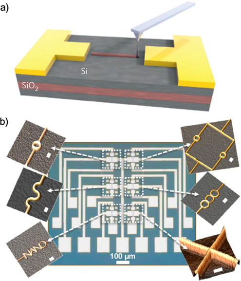
Silicon wafer substrates can be used for sample substrates, making systems (nano and microelectrical and mechanical MEMS ) . A useful flat substrate made of silicon wafer particles linked with nanowires and for biological applications, Si (silicon wafer) and making systems (nano and microelectrical and mechanical MEMS ) has properties similar to glass and can be mounted or grown Use nano wire particles. It can be easily erased or used as a whole wafer to reproduce and build systems (nano and microelectrical and mechanical MEMS ) .Systems (nano and microelectrical and mechanical MEMS ) silicon nanowire arrays or SiNWs are vertical arrays of silicon nanowires on a flat crystalline silicon wafer substrate. These nanowires are made by a catalytic oxidation and dissolution of Si in the presence of metal catalyst nanoparticles - a self-organized process commonly known as silicon wafer-assisted metal-chemically reinforced process .
Conclusion :
Silicon dioxide is used to prepare and build systems (nano and microelectrical and mechanical MEMS ) . The remaining photoresist is used as a hard mask that protects the silicon dioxide part. Photoresist is removed by wet etching ( hydrofluoric acid, sulfuric acid and hydrogen peroxide) or dry etching (using oxygen plasma). The result is a thin film of silicon dioxide on a silicon base.
Researcher and author: Dr. ( Afshin Rashid)
Specialized doctorate in nano-microelectronics


