UTS MOSFET based field effect nanotransistors (PhD in nano-microelectronics)
Researcher and author: Dr. ( Afshin Rashid)
Note: All nanotransistors on a wafer turn on and off at the same time because they have the same gate. The thickness of the oxide layer is high and on the other hand the production process is such that the contact surface of carbon nanotubes with the gate oxide is low. Low voltage parts cause problems.
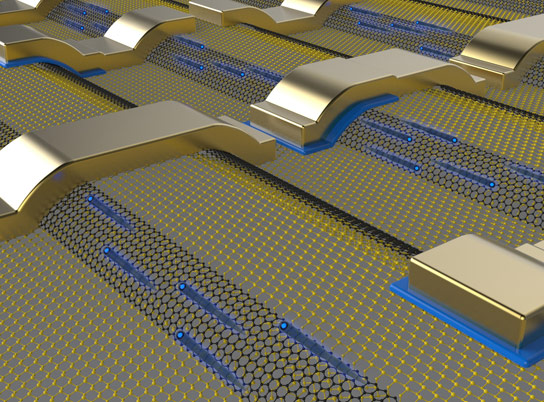
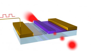
In the structure of high gate nanotransistors , carbon nanotubes are completely inserted into the gate insulation for greater gain. Unlike the field effect transistors of carbon gate nanotubes, many of these transistors can be built on a single wafer. , Because the gates of each are separate. Also, due to the low dielectric thickness of the gate in the nanotransistor, a larger electric field can be created with a low voltage on the carbon nanotube. Despite the more sophisticated manufacturing process than rear field gate carbon nanotube effect transistors, the above advantages make this type preferred.
Placing the gate around and on all the nanotubes, which improves the performance. Separating the source and drain area, si is added under the carbon nanotube. This removal continues until the bed insulation is reached. Then, using materials that have a high dielectric coefficient, insulation is created between the gate and the source and drain, and also a metal is placed on this insulation for better connection of the gate metal to the carbon nanotube.
Conclusion :
The process of making nanotubes has caused variability in the diameter of the tubes, which is usually between 1 and 2 nanometers. By changing the diameter of the nanotube, the band gap changes, and as a result, the transistor threshold voltage and the transistor current change.


