The density of electric charge increases in different regions (nano-transistors) or in other words, the number of electrical charges per unit area of nano-transistors increases (PhD in nano-microelectronics)
Researcher and author: Dr. ( Afshin Rashid)
Note: Nano-Microelectronics introduces new methods for making nanotransistors on a small scale, measuring several tens of nanometers, which is derived from a science called nanotechnology.
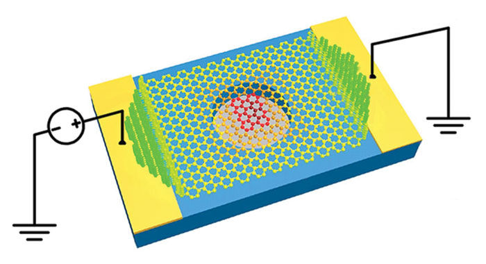
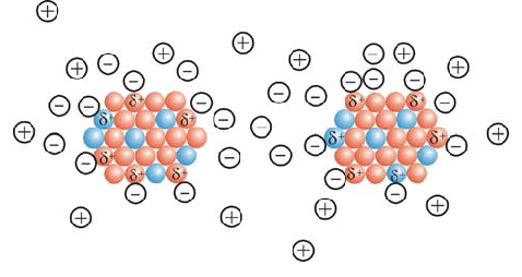
Unlike today's nanotransistors, which act on the mass motion of electrons in matter, new devices follow the phenomena of nanoscale quantum mechanics in which the discrete nature of the electron can no longer be ignored. By shrinking all the horizontal and vertical dimensions of the transistor, the electric charge density in the various regions of the nanotransistor increases, or in other words, the number of electrical charges per unit area of the nanotransistor increases. This has two negative consequences : First, by increasing the density of the electric charge, the possibility of discharging the electric charge from the insulated areas of the transistor increases, and this event causes damage to the transistor and its failure. This is similar to the discharge of excess electric charge between the cloud and the ground in the phenomenon of lightning, which ionizes air molecules into negative and positive ions. Secondly As the density of the electric charge increases, the electrons may move out of the radius of one atom and into the radius of the adjacent atom under the influence of the momentum or abduction forces that have now increased. This is called tunneling in quantum physics. Electron tunneling from one atom to an adjacent atom is a phenomenon that occurs on a small scale between electrons. This phenomenon is the basis of some electronic components and some nanoscopes. But in nanotransistors, this is not a useful phenomenon, because the tunneling of electrons from one atom to an adjacent atom may continue and cause an electric current. Although this electric current may be very small, because it is unintended and unpredictable, it behaves like a leakage path for electric current. And changes the electrical behavior of the nanotransistor.
We divide these devices into three parts:
1) Carbon nanotube tezansistors
2) Single electronic devices
3) Molecular nanoelectronic devices
Using nano-wire as a metal-oxide-channel semiconductor field A nano-effect transistor can enable a structure around a gate to perform an excellent electrostatic gate control over the channel to reduce short-channel effects. Which has been in the structure of nanocircuits and the basis of electronic nanoparticles for computing devices.


