

Section (Self-organized electrical nanostructure)
Self-organized electrical nanostructure and one-dimensional nanostructures, the possibility of improving the electrical-optical properties of nanoelectronic parts
Researcher and author: Dr. ( Afshin Rashid)
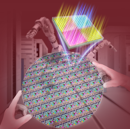
Note: Examining the band gap structure of nanoelectronic devices, in addition to introducing a method for researching the performance of one-dimensional systems, has made it possible to improve the electrical-optical properties of electronic components.
Devices based on organic materials can be mechanically flexible to a large extent due to the loose intermolecular bonds in the nanoelectrons created from them . Unlike these organic materials, minerals such as silicon, germanium, and gallium arsenide can only be used in the structure of electronic devices in crystalline states, and in this case, covalent bonds make flexibility impossible. Properties such as strength, flexibility, electrical conductivity, magnetic properties, color, reactivity, etc. Starting to change the properties of the material by shrinking it depends above all on the type of material and the desired property. For example, by reducing the dimensions of a material, generally some mechanical properties of the material such as strength are improved. This increase in strength does not happen only in the range of a few nanometers, and the strength of materials of several tens or even hundreds of nanometers may be much higher than the mass material of a large scale. On the other hand, the change of some properties such as color and magnetic properties may occur in dimensions of only a few nanometers.
In addition to these two cases, the state of energy levels of electrons around each atom and the number of electrons in its last layer are also influential in determining the properties of that atom or substance. This feature can play a decisive role in the mechanism of combining chemical properties of that substance. For example, the properties of a metal ion are different from the metal atom. Until now, the role of three factors, atomic number, mass number and electronic arrangement of the material is effective in determining the properties of the electrons of the nanostructure of the material. Macroscopic properties of a material such as melting point, boiling point and electrical conductivity, through the study of a sample that is sufficient to measure in the usual conditions of nanoparticles. This is not true for all materials, when the material size is reduced and reaches nanometer dimensions, completely different behavior and properties may be seen compared to the same material in large dimensions.
Define an instance
If a substance with a band gap structure of nanoelectronic devices and with a scale of several tens of meters is reduced to millimeter dimensions, there will be no change in its melting point, color and magnetic properties, but this change occurs when the material is reduced to dimensions nanometer is seen and the number of surface atoms in materials with scales larger than nanometers is very small, but upon entering the nanometer world, the amount of these atoms increases greatly compared to the total atoms of the material.

Conclusion:
Examining the band gap structure of nanoelectronic devices, in addition to introducing a method for researching the performance of one-dimensional systems, has made it possible to improve the electrical-optical properties of electronic components.
Researcher and author: Dr. ( Afshin Rashid)
Specialized doctorate in nano-microelectronics