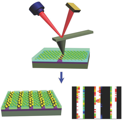
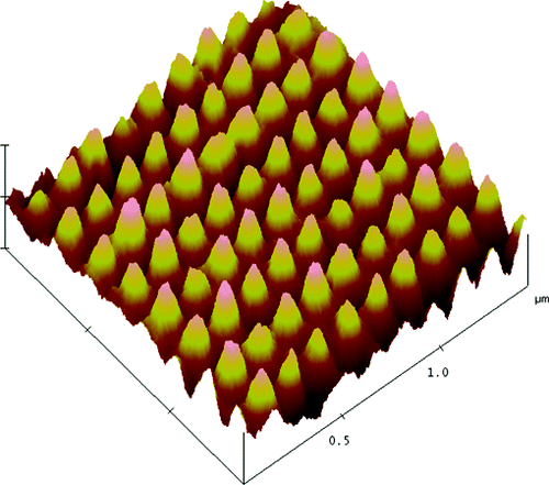
Plasmonic nano-lithography (90 nm) and fabrication of nanoelectronic devices (PhD in nano-microelectronics)
Researcher and author: Dr. ( Afshin Rashid)
نکته: نانو لیتوگرافی با چگالی بالا را با استفاده از پلاسمون های سطحی بر روی یک بستر آلومینیومی سوراخ شده با آرایه های دو بعدی با استفاده از یک منبع نور UV (یو_وی) نزدیک به منظور برطرف کردن ویژگی های طول موج فرعی با انتقال زیاد انجام می شوند.
Optical nano- lithography has played a major role in the development of the semiconductor industry in the last few decades due to its high efficiency. The lithographic methods currently used in the manufacture of nano-electronic scale devices are mainly based on optical technology using equipment that is widely used in many industrial processes. Optical lithography has advanced by pushing the optical resolution limit to produce high-density electronic devices. Optical sharpness, which reflects the imaging performance of an optical lithography system, is limited by the inherent characteristic of light diffraction.
Extraordinary transmission of light through a metal perforated film offers new possibilities for high-intensity optical lithography near the field produced by nano-diaphragm metal. Lithographic systems using such high-resolution nano-aperture transitions have achieved below-resolution diffraction, and have begun developing new designs of plasmonic nanolithography. To achieve high optical resolution, the distance between the aperture and the image resistance must be exactly within Save a few tens of nanometers, because the field connection is very sensitive to close distances. In addition to this difficulty, a major drawback of near-field lithography is the lack of modeling power.For rapid nanoscale modeling, molecule properties are performed by contact printing, parallel processes with console two-dimensional arrays or flexible polymer pen arrays for plasmonic nano-lithography (90 nm), and fabrication of nanoelectronic devices, a parallel process with a The font array was only intended for an array pattern of the same structure, because each array font could not be activated separately. To generate nanoscale patterns on a larger scale, we need a probe array whose elements are activated separately. Using an array of nano-aperture probes in a parallel process is a promising way to achieve high-power, near-field optical lithography. However, in practice, it is difficult to implement an array of optical probes that hold thousands or millions of elements close to capture the field, because the distance between each probe and the pattern bed must be accurately maintained in the tens of nanometers. Each optical probe has an additional layer of solid film below the diaphragm so that it can physically contact the substrate and maintain gap spacing during the scan.
Conclusion :
High-density nano-lithography is performed using surface plasmons on a perforated aluminum substrate with two-dimensional arrays using a near-UV light source to eliminate high-transmission sub-wavelength characteristics. .
Researcher and author: Dr. ( Afshin Rashid)
PhD in Nano-Microelectronics


