Planar FET nanotransistors (PhD in nano-microelectronics)
Researcher and author: Dr. ( Afshin Rashid)
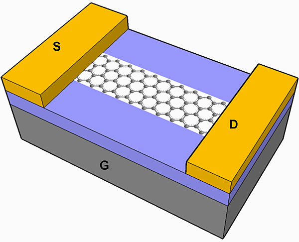
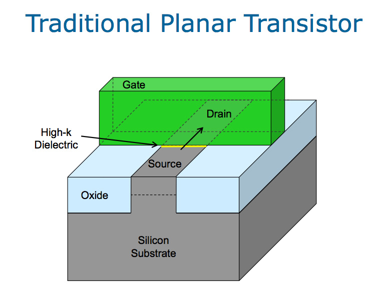
Note: Planar FET nanotransistors are a flat structure, consisting of three components: a gate, a collector, and a base or gate, which control the flow of electrons between the two by nanowires.
Planar FET nanotransistors are responsible for the total current of electrons in a thin nanoplay under the gate, called the inversion layer, and a fine nanowire acts between the two poles of an electrical outlet. This was not a problem when transistors were measuring 180 nanometers or more, but as they shrank, the inverted nanofilm became thinner and thinner and less efficient. As a result, even when the transistor is off (gate leakage), more energy and current flows between the current and collector, and the voltage difference between the two states is smaller.
By reducing gate leakage through technologies such as nanowires, Nano wire reduces the voltage difference across the gate, forcing more electrons to pass through the inverting nanostructure, reducing the voltage difference problem in Planar FET nanotransistors, and The result is a much larger contact area and better control of electron flow. Because there are now three points between the nanolayer inversion layer and the contact gate of Planar FET nanotransistors, transistors based on Planar FET nanotechnology make contact with a single gate at three points, even if the logic performance is the same. .
Conclusion :
Planar FET nanotransistors are a flat structure, consisting of essentially three components: an emitter, a collector, and a base or gate, which control the flow of electrons between the two by nanowires.


