- Nanoelectronics and the effect of quantum confinement
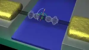
Nanoelectronics and the application of quantum tunneling nanostructures in the formation of resonant nanodiodes (Si and Gi)
Researcher and Author: Dr. ( Afshin Rashid)
Note: In nanoelectronics technology, substrate surface processes (Si and Gi) such as burning are performed by plasma and ion beam technology. Such integrated circuits with their unique features at the nanometer scale have diverse applications in (mesoscopic) systems.
Characterization of Si/Gi multilayer systems has recently been investigated in the field of the effect of negative bias voltage on improving the nanoelectrical and structural properties of the Ta sputtering layer in the Si/Ta nanosystem. Also, in the technology of designing nanoelectronic components, using and fabricating the thin layers required in the aforementioned integrated circuits is only possible in environments defined by precise deposition methods such as molecular beam deposition (MBE) and metal organic chemical vapor deposition (MOCVD).
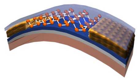
Basically, semiconductor-metal junctions are an essential part of all nanoelectronic devices. The nature and behavior of nanoelectrical junctions depend on the surface concentration of semiconductors (Si) and (Gi), the cleanliness of the surface, and the reactions between the metal-semiconductor interface. After the invention of the nanotransistor, the concept and importance of integrated circuits became clear. After that, the great success of assembling and connecting a large number of small parts and electronic components on the surface of the substrate created a huge revolution in the practical manufacture of integrated circuits. With the invention and development of the technology of miniaturization of nano-microelectronic devices, the use of quantum tunneling nanosystems in nano-resonant diodes (Si and Gi) and other nano-devices is possible.

With the development, design and manufacturing of integrated nanocircuits, especially the increase in the accumulation of components on a very large scale and the effort to make microelectronic components smaller continued. On the other hand, the new demand for the manufacture of integrated circuits, especially memory nanocircuits including dynamic nanomemory (DRAM) and static memory (SRAM) with features such as high operating speed combined with reduced power dissipation, has increased day by day . In the evolutionary process of the technology of ultraminiaturization of nanoelectronic components, especially in the submicron geometry and scale of less than 2.0 μm, that is, the field of nanoelectronic component design technology and manufacturing technology based on Gi and Si nanostructures, integrated nanocircuits have a certain complexity.
Conclusion:
In nanoelectronics technology, substrate surface processes (Si and Gi) are performed, including burning by plasma and ion beam technology. Such integrated circuits with their unique features at the nanometer scale have diverse applications in (mesoscopic) systems.
Researcher and Author: Dr. ( Afshin Rashid)
Specialized PhD in Nano-Microelectronics


