

Nano Wires ( NWS) Doped
Researcher and author: Dr. ( Afshin Rashid)
Note: Nanowires ( NWS) alone cannot control the movement of electrons, so impurities must be added in a process
called doping, usually with boron, phosphorus, selenium, or germanium.
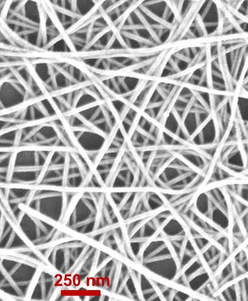
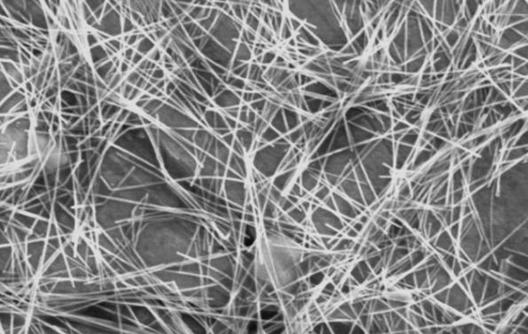
When the nano wire is doped, the motion of the electrons can also be converted, allowing the electron current to be turned on or(electron flow stop), using the voltage between the nanowire layers (NWs) on and off. Turns off. Another nanostructure that has been the subjectof muchstudy andresearchtodayis nanowires. A wire is generally a structure that extends in one direction (longitudinal direction) and is very limited in the other two directions . An essential feature of these structures, which have two outputs, is electrical conductivity. Electrical charge transfer occursby applying a differencein electricalpotential at both ends of these structures and along their length.Making wires in nanometer dimensions is very interesting both technologically and scientifically, because in nanometer dimensions they have unusual properties . The length to diameter ratio of nanowires is very high (metal nanowires). These nanostructures are due to their special properties. Which promise great performance in electronic components. Metal nanowires are one of the most attractive materials due to their unique properties that lead to their various applications . Nanowires can be used in computers and other computing devices. To achieve complex nanoscale electronic components, we need nanoscale wires. In addition, nanowires themselves can be the basis of electronic components such as memory.
(Organic nanowires) These types of nanowires, as their name implies, are derived from organic compounds. In addition to metallic and semiconductor materials, it is also possible to make nanowires from organic materials. Recently, a substance called "oligophenylene vinyl" has been developed for this purpose. The characteristics of these wires (such as conductivity and resistance and thermal conductivity) depend on the structure of the monomer and its arrangement. The chemical structure of these compounds gives rise to interesting properties. The future of nanotechnology depends on the ability of researchers to acquire techniques for organizing molecular components and nanometer structures. By imitating nature, they organize the dough proteins to produce conductive nanowires. Organizing living components in nature is the best and oldest example of "bottom-up" construction, and therefore it can be used to understand and find ways to make electronic and micrometer devices. Until now, "top-down" manufacturing techniques have been used, which are often laborious and costly at the nanometer scale, and the commercialization of nanotechnology requires easy and cost-effective methods, the best example of which is the nature around us; All we have to do is open our eyes a little and look around more carefully. (Silicon nanowires) This type of nanowire is non-toxic and does not damage cells. This type of nanowires has shown its greatest application in the medical field, such as detecting cancer symptoms, stem cell growth, etc. , which we will discuss below.

Conclusion :
Nanowires ( NWS) alone cannot control the movement of electrons, so impurities must be added in a process called doping, usually with boron, phosphorus, selenium or germanium.
Researcher and author: Dr. ( Afshin Rashid)
PhD in Nano-Microelectronics