Field Effect Nano Transistors (Nano Teransistor Mosfet)
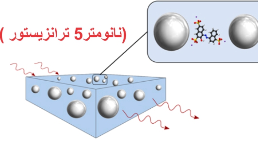
Nano Gate Transistor - Gate around ( 5 nm transistor)
Researcher and author: Dr. ( Afshin Rashid)
Tip: A gate nanotransistor - the gate around the FET - can get around the problem. And in terms of electrostatics, an all-gate gate is a nanotransistor in which a gate is placed on all four sides of the channel. It is basically a silicon nanowire around which the gate rotates. In some cases, the surrounding FET can have a common gate or other material in the channels.
Horizontally layered nanolattices appear as the consensus for the 5nm transistor. These devices start with alternating layers of silicon and silicon germanium (SiGe) that are patterned into pillars. The creation of the initial Si/SiGe heterostructure is straightforward and the columnar pattern is similar to the fin structure for nanotransistors. However , for GAAFET nanosheet transistors, the indentation in the SiGe layers creates an internal gap between the source/drain, which ends up next to the pillar and the gate space of the nanotransistor. This opening distance determines the width of the gate. Then, once the internal spacers are in place, an etch removes the free SiGe channel.
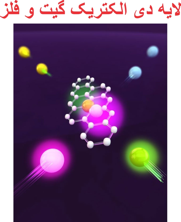
In the gate-gate nanotransistor structure , the dielectric nano layer of the gate and the metal is placed in the spaces between the silicon nanowires around ( 5 nm transistor) . To minimize lattice distortion and other defects, the germanium content of SiGe layers should be as low as possible. The selectivity of the nano layer in the surrounding gate nanotransistor increases with the content of Ge or germanium, and the erosion of the silicon layers during the indentation of the inner gaps or the gate of the nano transistor release channel and the channel affects the thickness of the gate channel around and thus the threshold voltage. put
Conclusion :
Horizontally layered nanolattices appear as the consensus for the 5nm transistor. These devices start with alternating layers of silicon and silicon germanium (SiGe) that are patterned into pillars. The creation of the initial Si/SiGe heterostructure is straightforward and the columnar pattern is similar to the fin structure for nanotransistors.


