

Section _ reproduction and production of nanowires
Investigating and analyzing the processes of nanowires reproduction on silicone wafers
Researcher and author: Dr. ( Afshin Rashid)
_yzl.gif)

Note: Silicone wafers For biological applications, silicon is similar to glass, which makes it a suitable support for the growth and/or nanoparticle mounting of nanowires. For nanoelectronics applications, it is an ideal sample substrate for small nanoscale particles due to its low background signal and highly polished surface.
Silicon wafer substrates can be used for sample substrates, microfabrication, substrates for nanowires or biological substrates. A useful flat bed of silicon wafer particles linked with nanowires and for biological applications, Si (silicon wafer) has properties similar to glass and can be used to mount or grow nanowire particles. It can be easily wiped off or used as a whole wafer for the propagation of nanowires.
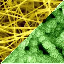
Silicon nanowire arrays or SiNWs are vertical arrays of silicon nanowires on a flat crystalline silicon wafer substrate. These nanowires are made by a catalytic oxidation and dissolution of Si in the presence of metal catalyst nanoparticles - a self-organized process commonly known as silicon wafer- assisted metal-chemical enhanced process.
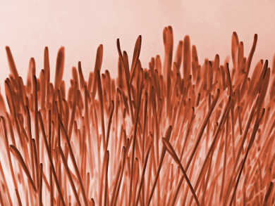
The processes used to reproduce nanowires on silicon wafers make Si Nanowire arrays more reproducible and uniform, and allow the properties of nanowires to be tuned. The propagation process of nanowires always involves the deposition of a metal and bonding in a solution containing hydrofluoric acid (HF) and an oxidizer. Silicon is produced only where metal nanoparticles touch silicon, as a result of electrochemical reactions with the help of nanoparticles, as silicon is carried, the nanoparticles move into the resulting nanoparticles. Since silicon is only locally doped, this process can lead to very high aspect ratio features in nanowires.

Conclusion:
Silicon wafers For biological applications, silicon resembles glass, which makes it a suitable support for the growth and/or nanoparticle mounting of nanowires. For nanoelectronics applications, it is an ideal sample substrate for small nanoscale particles due to its low background signal and highly polished surface.
Researcher and author: Dr. ( Afshin Rashid)
Specialized doctorate in nano-microelectronics