

_ Nano assemblers in the manufacture of new electronic nano devices
Nano-assemblers and electrical nano- arrays ( spin-qubits)
Researcher and Author: Dr. ( Afshin Rashid)
Note: Applications of nanoassemblers include data storage nanodevices or nanomemories , single-electron nanotransistors, and spin-qubit nanoarrays for quantum computing.
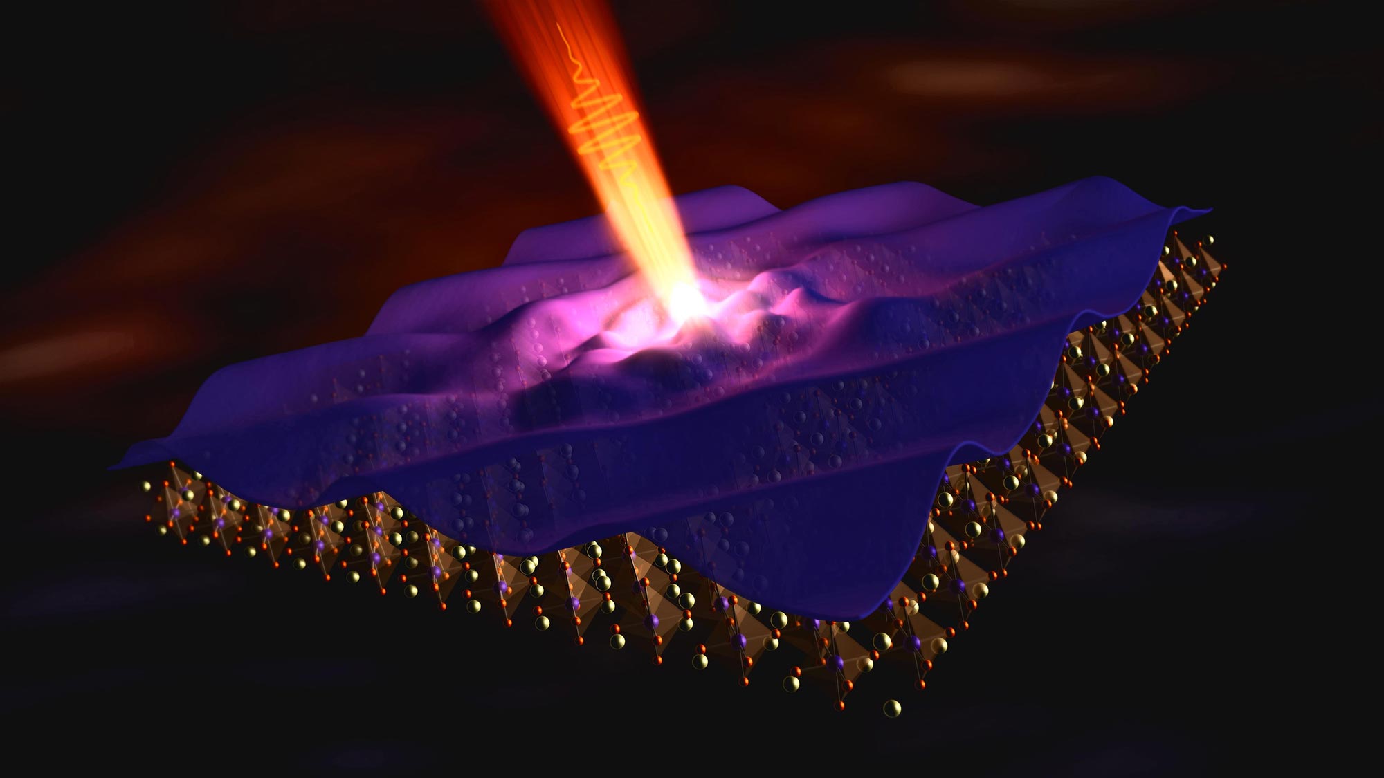
With the advent of the new nano-microelectronics technology, the precision of device manufacturing devices has not improved in line with the shrinking dimensions of spin-qubit arrays . In smart nanostructures, the concept of nano-assemblies is summarized in all the information and codes necessary to produce an identical entity. We have a very small machine that knows how to produce its own counterpart , which in nanoscience is referred to as a "nano-assembler". Nano-assemblers are composed of nanoparticles, and the first effect of reducing particle size is to increase the surface area. Increasing the surface area to volume ratio of nanoparticles causes the atoms located on the surface to have a much greater effect on the physical properties of the particles than the atoms within the particle volume. This feature greatly increases the reactivity of nanoparticles. The structure of nano-assemblers is one of the properties of nanoparticles, the high surface area to volume ratio of these materials. Using this property, powerful catalysts can be produced in nanometer sizes. These nanocatalysts will greatly increase the efficiency of chemical reactions and will also significantly prevent the production of waste materials in the reactions. The use of nanoparticles in the production of other materials can increase their strength or reduce their weight. It can increase their chemical and thermal resistance and change their reaction to light and other radiation. By using nanoparticles, the strength-to-weight ratio of composite materials will increase greatly.
To form nanoassemblers and nanoarrays (spin-qubits ) in nanoelectronics, modified raw materials are needed (transistors and diodes), and every material around us has a unique energy structure for electrons, and the energy structure of different materials is different from each other. According to nanoelectronics, in an atom, electrons can only occupy certain atomic orbitals with discrete energy levels. If several atoms are placed together to form a molecule, their atomic orbitals are split due to the effect of the nuclei of each atom on the electrons of all atoms and the Pauli exclusion principle. When a very large number of atoms are placed together to form a crystal, the number of orbitals increases tremendously and as a result their energy levels come close to each other. So that the energy levels appear continuous. In this case, instead of energy levels, bands or bands of allowed electronic energy are formed . Between these bands are forbidden gaps, where electrons similar to discrete levels in the atom cannot fit into this gap. In macroscopic and ordinary materials, it consists of energy bands. In different atoms, the distance between the levels is different, and in ordinary cases, the width of the energy bands and the width of the forbidden region (energy gap) are different from each other.

Conclusion:
Applications of nanoassemblers include data storage nanodevices or nanomemories , single-electron nanotransistors, and spin-qubit nanoarrays for quantum computing.
Researcher and Author: Dr. ( Afshin Rashid)
Specialized PhD in Nano-Microelectronics