

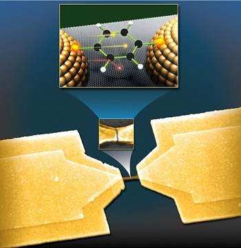
_ Nano assemblers in the manufacture of new electronic nano devices
Nano Assemblers and (III-V) compounds are the main factor in the emergence and creation of electrical nanodevices such as nanodiodes.
Researcher and Author: Dr. ( Afshin Rashid)
Note: (III-V) compounds are the main factor in nanodevices such as nanolight-emitting diodes. Determining this spectrum is the energy gap in the semiconductor used.
There is no other way to change the energy gap than to use semiconductor compounds instead of semiconductor elements. A few decades ago, LEDs with two light spectra, red and green, were made, but the possibility of making blue nano-LEDs with high brightness remained an unsolvable puzzle. Making LEDs with a blue light spectrum using GaN made it possible to produce white light with LEDs. Some of the nano-LED lamps are the most efficient lamps that are increasingly used. Photodetectors are key components of these circuits. The main substrate for making these circuits is photonic crystals. Compounds (III-V) of nano-optical and nano-optical devices are among the most widely used nano-microelectronics. Currently, the possibility of connecting between silicon processor cores and peripheral memory by integrated optical communication channels made of compound semiconductors, with very high data transfer rates in other communication and connection technologies between processors, has attracted integrated optical nano-electronics.
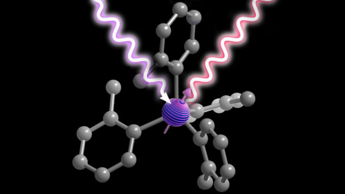
III-V compounds Apart from some elements of group 4 of the periodic table, namely Si and Ge, which are semiconductors, compounds of elements of group 3 with 5, group 2 with 6, and also alloys of group 4 with 4 also have semiconductor properties. Even some compounds of three elements of these groups, such as AlGaAs and InGaN, also have semiconductor properties. At the beginning of the recognition of these compounds and research on them, it was thought that they would soon replace silicon, because it was possible to engineer and obtain some properties that were not present in silicon. However, due to the lack of a suitable insulator for use in the gate of transistors and the high cost of the elements and the deposition process of compound semiconductors V-III, silicon and finally the silicon-germanium alloy still remain as the main semiconductor used. It should be noted that silicon oxide, which can be easily deposited with high purity, is a very suitable insulator for this purpose. Today, in integrated circuits with channel lengths below 50nm, alternative oxides with higher dielectric constants such as zirconium oxide ZrO2 and hafnium oxide HfO2 are used. In ternary alloys, different properties of the semiconductor can be obtained by changing the ratio of the two elements present. For example, in xAs-AlxGa1 and xN-InxGa1, changing x leads to a change in the energy gap and many of the properties of these semiconductor compounds are due to the band energy structure. The (III-V) compounds find nano-optical devices (xAs-AlxGa1) in the (45.0<x) state, along with changes in the distance between the valence band edge and the conduction band edge with changing x in three different directions of wave propagation.

Conclusion:
Researcher and Author: Dr. ( Afshin Rashid)
Specialized PhD in Nano-Microelectronics