

_ Nanoplasmonics and nanoelectronics pattern section
Introducing (nanoplasmonics and nanoelectronic patterning) one of the miniaturization techniques in the design of nanodevices such as nanologic gates
Researcher and Author: Dr. ( Afshin Rashid)

Note: Micro/nano patterning is one of the techniques for miniaturizing patterns, especially for electronics. Today, soft lithography has become a standard in biomaterials engineering and fundamental research in cell biology. It generally uses lithography methods, but many techniques have been developed. Batch fabrication of microstructures requires a low-cost, high-throughput surface patterning technique.
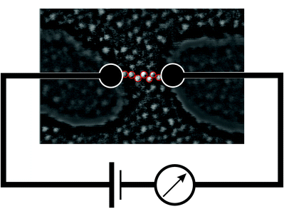
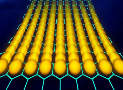
Micro/nano patterning is one of the techniques for miniaturizing patterns in the design of nanodevices such as nanotransistors and nanodiodes, nanoswitches and nanologic gates, in order to design nanoscale computers with dual-scale capabilities. All living biological systems function due to molecular interactions of different subsystems. Molecular building blocks (proteins and nucleic acids, lipids and carbohydrates, DNA and RNA) can be considered as an inspiring strategy on how to design high-performance NEMS and MEMS that have the required features and characteristics. In addition, analytical and numerical methods are available to analyze the dynamics and three-dimensional geometry, bonding and other features of atoms and molecules. Thus, electromagnetic and mechanical, and other physical and chemical properties can be studied.
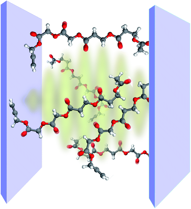
Nanostructures and nanosystems can be widely used in medicine and healthcare. Possible applications of nanotechnology include: drug synthesis and drug delivery (the therapeutic potential is greatly increased due to the effective direct delivery of new types of drugs to specific sites in the body), nanosurgery and nanotherapy, genome synthesis and diagnostics, nanoscale actuators and sensors (diagnosis and prevention of disease), design and implantation of non-removable artificial organs, and design of high-performance nanomaterials. It is important that these technologies change the manufacturing and production of materials, devices, and systems.
Nanostructures are used in combination to bend in response to the application of an electric voltage. The use of nanostructures is widespread in a wide range of industries and consumer products. In nanoscience , the structure of materials determines the relationship between the atoms, ions, and molecules that make up those materials. To understand the structure of materials, one must first understand the type of connections between atoms and ions . Chemical bonds determine the way atoms and ions are connected. Therefore, the difference between the types of connections can be seen in the characteristics of these bonds. Of course, it is important to note that the intensity of the electromagnetic field (specifically the intensity of the electric field) decreases exponentially as one moves away from the surface of the metal nanoparticle. In this created nanovolume, the electromagnetic field is localized, compressed, and enhanced.

Conclusion:
Micro/nano patterning is one of the techniques for miniaturizing patterns, especially for electronics. Today, soft lithography has become a standard in biomaterials engineering and fundamental research in cell biology. It generally uses lithography methods, but many techniques have been developed. Batch fabrication of microstructures requires a low-cost, high-throughput surface patterning technique.
Researcher and Author: Dr. ( Afshin Rashid)
Specialized PhD in Nano-Microelectronics