FinFET nanotransistor scale reduction causes more short channel effects, less gate control, increased leakage current exponentials, severe process changes and uncontrollable power densities (PhD in Nano-Microelectronics)
Researcher and author: Dr. ( Afshin Rashid)
Note: Because FinFEET nanotransistors achieve a larger discharge current in the nanotransistor , the channel width with respect to the height as well as the thickness, which the nano-CNTs layers keep in the smaller range.
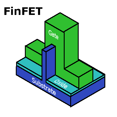
FinFEET nanotransistors A nanotransistor ( metal-oxide-semiconductor field effect ) built on a substrate . The gate is located on two, three or four sides of the canal or is twisted. The canal forms a double gate structure. These devices are commonly called "finfets" because the source / discharge area forms fins on the silicon surface. FinFET devices have significantly faster switching and higher current densities than flat technology, using nanowires (metal oxide and semiconductor complement) in the structure .
Due to the scale reduction of semiconductor components and integrated circuits up to the nanometer range, in FinFET nanotransistors scale reduction causes more short channel effects, less gate control, increased leakage current exponentials, severe process changes and unmanageable power densities. Between the carbon and metal nanotubes used to connect the source and the drain, a FinFET nanotransistor forms the Schottky barrier (SB). The formation of Schottky dams in the source and drain sections of a transistor significantly reduces the current flow in these FinFET nanotransistors. Therefore, for higher operational efficiency of Finfet nanotransistor components, suitable metals are needed that can be used at the source connection and in the nanotransistor to create an ohmic connection. The ability of carbon nanotubes to be used in FinFET nanotransistors is hollow and high. Being their contact level. In FinFET nanotransistors, when an electric field is applied , the carbon nanotube between the source and the drain contains a moving charge . The density of these loads is for the source , and this density is electrically distributed in the multilayer nanotubes for which there is also the possibility of a Dirac form distribution.


