

Electric properties in the self-organized DND electric nanostructure (Electric as properties)
Researcher and author: Dr. ( Afshin Rashid)

Note: Nanostructures can be defined as materials that have at least one external dimension with a size of 1 to 100 nm. And the particle size of at least half of the particles in the number size distribution must be 100 nm or less. Nanostructures can occur naturally, be created as byproducts of combustion reactions, or be purposefully produced through engineering to perform a specific function. These materials can have different physical and chemical properties from their original bulk samples.
Nanostructures are used to bend in a composite manner in response to the application of electric voltage . The use of nanostructures is widespread in a wide range of industries and consumer products. In nanoscience, the structure of materials determines the relationship between atoms, ions and molecules that make up those materials. To understand the structure of materials, one must first understand the type of connections between atoms and ions . Chemical bonds determine how atoms and ions are connected. Therefore, the difference between different types of connections can be seen in the characteristics of these links.
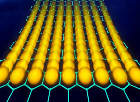
Nanostructures Nano structure The electronic properties of the two regions are "protected" by a special, so-called topological, different method. And therefore, a new very strong quantum state is created in the transition region. This localized electronic quantum state can now be used as a key feature to produce certain semiconductors, metals or insulators – and possibly even as a feature in nanoelectronics. The shapes and sizes of nanostructures are naturally determined based on their composition and formation conditions. The characteristics of the nanostructures, in turn, determine the originality of the characteristics of the nanostructures and their possible fields of operation. The range of 1 to 1000nm is introduced as the range of nanostructures, the important feature of nanostructures is to control the processes of the organization itself. The range of nanostructure activity change depends on the nature and shape of the nanostructure. However , if the energy of the nanoparticle field is comparable to the energy of electromagnetic radiation and if significant changes are made in a certain wavelength range with the occurrence of chemical reactions in the irradiated materials, the activity of nanoparticles up to 100nm will be significant.

Conclusion:
Nanostructures can be defined as materials that have at least one external dimension with a size of 1 to 100 nm. And the particle size of at least half of the particles in the number size distribution must be 100 nm or less. Nanostructures can occur naturally, be created as byproducts of combustion reactions, or be purposefully produced through engineering to perform a specific function. These materials can have different physical and chemical properties from their original bulk samples.
Researcher and author: Dr. ( Afshin Rashid)
Specialized doctorate in nano-microelectronics