

_ Section (Self-organized electrical nanostructure
DND electrical nanostructures are an example of the proliferation of nanoparticles in the active medium
Researcher and author: Dr. ( Afshin Rashid)
Note: The nanostructure of DND is an example of the multiplication of active wires, there is no problem to produce it like polymers, only its properties should be investigated to understand how it changes.
DND is an example of active wires. The structure of DND is well known and automatically this structure is created in the propagation of nanowires. In order to use DND to calculate the current in terms of voltage, a distance of 8 nm between two platinum electrodes is assumed, so by applying a voltage, the current can be calculated. The point that can be taken from the reaction is that the current diagram in terms of voltage is an asymmetric diagram, that is, the current is not allowed to pass for a voltage between 1 and 2 volts, for example, while it can pass for a current of 2 and 1, and this means That DND can do the rectification.

There are three theories about conduction inside DNA, one is that DND is a semiconductor with a very large gap. Another thing is that DND is a semiconductor with a small gap and also that DND has metallic properties. The main issue is that DND is a very complex substance that environmental conditions can greatly affect its properties. One of these effective environmental conditions is the presence of water, DNDs in a dry environment with DNDs in a wet environment. It is very different. Therefore, according to the local conditions governing DND, it is not possible to make a definite conclusion about whether DND is metal or semi-metal, but what is certain is that DND is a semiconductor with a large gap. Normally, there are ions that can be manipulated to change the conductive properties of DND, that is, it can be hoped that by adding ions it can even be turned into a metal. Another interesting point is that DND can be used as a template and in At specific places on the DND, he placed series of metals to form a metal wire around the DND. In this case, DND is used as a template to keep the desired wire stable.
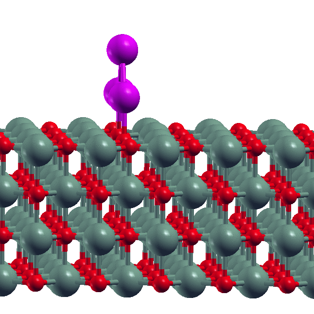
Checking the stability of DND according to the local conditions governing the system is also possible. DND guidance takes place in two specific ways. When DND is considered as a current conductor, once it can pass the current in the direction parallel to its axis and once it can pass the current perpendicular to its axis. STM carbon nanotube molecule is placed on top of the DND, the current enters the tip of the STM in a perpendicular form from the available pairs, this work can be used both as an experiment to see the image of the DND and to measure the passage of the current of the pairs, and it can be used in this way Calculate the conductance of AT and CG (pairs of openings present in the DND helix). DND can be a tool in the production of nanoelectronic products with many applications, considering that DND exists naturally in nature and in the cells of living organisms, it can be used in the production of other nanotechnology products such as nanomotors. The control and stability of DND is also possible due to its inherent and local properties, and it is worthy of consideration and discussion.

Conclusion DND nanostructure is an example of the proliferation of active wires
1- What is certain, molecular electronics has a bright future and is growing and evolving at a very fast rate. Therefore, it requires special attention.
2- The practical results of the growth and development of nanotechnology branches such as nanoelectronics will lead to the construction of equipment that is vastly different compared to the past and will be a completely new generation with unique capabilities.
Researcher and author: Dr. ( Afshin Rashid)
Specialized doctorate in nano-microelectronics