

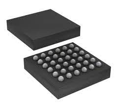
_ Understanding ( Micro BGA ICs) or (Micro Ball Base)
Examining the internal structure and construction of a micro BGA (memory holder or MEMORY) chip of the micro BGA or micro memory ball base type.
Researcher and Author: Dr. ( Afshin Rashid)

Note: A MEMORY IC (Ball-base or Micro BGA) is a "read-only" memory, a small chip that is placed on boards that contains information that the manufacturer fills in. The information inside this component may be executed multiple times, so it is of relatively significant importance.
The information stored in the MEMORY ic is read-only and users cannot erase, delete, or change its information.


The process of creating the initial template for micro BGA or ball-base MEMORY IC chips is difficult. However, the advantages of micro BGA or ball-base MEMORY IC memory outweigh some of its disadvantages. Once the template is completed, the prepared chip can be sold in bulk and at a low price. This type of memory uses little power, is reliable, and in most small electronic devices, contains all the necessary instructions to control the desired device. The use of this type of chip is widespread in some toys for playing music, laptops, tablets, and external hard drives.

The micro BGA uses a different approach than the one used in most common surface mount connections in the past. Other packages, such as the quad flat package (QFP), use the perimeter of the package for connections. This means that there is limited space for the pins to be close together and they must be very small to provide the desired level of connectivity. The micro BGA uses the bottom of the package, where there is significant space for connections. The micro BGA was developed due to the need for a stronger package that was more suitable for manufacturing integrated circuits with a high pin count.
Memory IC is required in almost every computing device to make it functional and functional. Micro BGA or ball socket MEMORY IC is a type of memory, the data stored in it remains, i.e., does not disappear after the user logs out of the system or reboots the system. This is possible due to the non-volatile nature of Micro BGA or ball socket MEMORY IC . Micro BGA or ball socket MEMORY IC is also referred to as secondary memory and is used as a storage medium in devices such as computers, mobile phones, IoT devices, etc. Micro BGA or ball socket MEMORY IC is an integrated circuit that is pre-programmed with specific functional data at the time of manufacturing. It is also called Firmware. These ROMs are not limited to computers. Most electronic gadgets make use of its flexible functionality.
- Researcher and Author: Dr. ( Afshin Rashid)
Specialized PhD in Nano-Microelectronics