

Department of systems (nano and microelectric and mechanical MEMS )
Classified processes such as: ( metallization)
Researcher and author: Dr. ( Afshin Rashid)
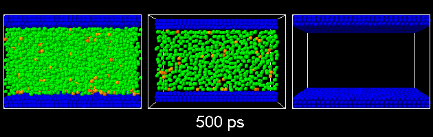

Synthesis and properties of metal nanoparticles is a major field in the construction of systems (nano and microelectrical and mechanical MEMS) . Especially the use of nanoparticles is very important in the applications of nanoelectronics technology, because when the size of the metal particles reaches the nanometer scale, it often shows optical, magnetic, electrical and chemical (catalytic) properties. The use of metal microparticles in decomposition is particularly interesting due to their irregular surface - which is continuously regenerated to adapt to the adsorbent - and their size-dependent electronic properties, which can be used to optimize catalytic activity and selectivity in The construction of systems (nano and microelectric and mechanical MEMS) should be regulated. Our group is able to synthesize a wide range of metal nanoparticles and metal oxide nanoparticles for applications in catalysts and in systems (nano and microelectric and mechanical MEMS) . A major challenge in the preparation of nanoparticle colloidal suspensions is stability, as they tend to aggregate to minimize surface tension. For this reason, the control of both nucleation and growth processes is very important to prepare stable monodisperse colloidal suspensions. In this context, there are several paths for the synthesis of nanoparticles, including chemical methods, metal vaporization, laser gas decomposition, gas phase methods, and plasma chemical reduction methods. We have successfully prepared sub-nanometer Pd particles that are first prepared in toluene (organosol) and, if desired, slightly transferred to the aqueous phase. This method allows obtaining aqueous solutions with a high concentration of dispersed Pd nanoparticles (44 mM) and stable suspensions over a long period of time (months).

Due to their wide application, nanoparticles are of great interest in and mechanical MEMS)systemsWhile natural materials have constant physical properties regardless of size, the size of a nanoparticle determines its physical and chemical properties. Therefore, the properties of a material change as its size approaches the nanoscale and the percentage of atoms on the surface of the material becomes significant. The important feature of all nanostructures is that the number of surface atoms in them is more than the number of volume atoms. This ratio increases with decreasing nanoparticle size. Therefore, the size of the nanoparticle is considered its most important feature. The range of activity of nanoparticles depends on the nature and shape of the nanostructure. With However, if the energy of the nanoparticle field is comparable to the energy of electromagnetic radiation, and if in a certain range of wavelengths, chemical reactions occur in the irradiated materials, significant changes are made, the activity of nanoparticles up to 100nm in the construction of systems ( Nano and micro electricaland mechanical MEMS)will be impressive.

Conclusion :
Two parameters are used to describe the structure ( metallization) in systems (nano and microelectric and mechanical MEMS) . One is Ch, which starts from the main atom of the chiralized vector and is directed towards the next atom, and it is also called the metallization vector , and its length is equivalent to the environment of (nano, micro , electrical and mechanical MEMS) systems .
Researcher and author: Dr. ( Afshin Rashid)
Specialized doctorate in nano-microelectronics