

Section (Self-organized electrical nanostructure)
Self-organized electrical nanostructure of DND in multi -layered nanostructures .
Researcher and author: Dr. ( Afshin Rashid)
Note: In nanoelectronics technology, special parameters and systems must be used to perform such processes. For example, in the metal marking process, it is inevitable to use copper metal instead of the common aluminum metal for internal connections between different practical parts. But the rapid penetration of Cu atoms under Si during heat treatment leads to the formation of a copper silicide layer and ultimately causes the destruction of the electronic component.
To solve this problem, they usually use an intermediate layer of retarding materials such as Ta and w or Mo as a penetration barrier to improve the thermal stability of the Si/Cu layer . In the characterization of nanoparticles and Si/Ta/Cu multi-layer systems, there is an effect of negative bias voltage on improving the electrical and structural properties of the permeation barrier of the Ta sputtering layer in the Si/Ta system. Surface processes of the Si layer, including burning, are carried out by plasma and ion beam technology. This kind of integrated circuits with their unique characteristics in the nanometer scale have various applications of mesoscopic systems.
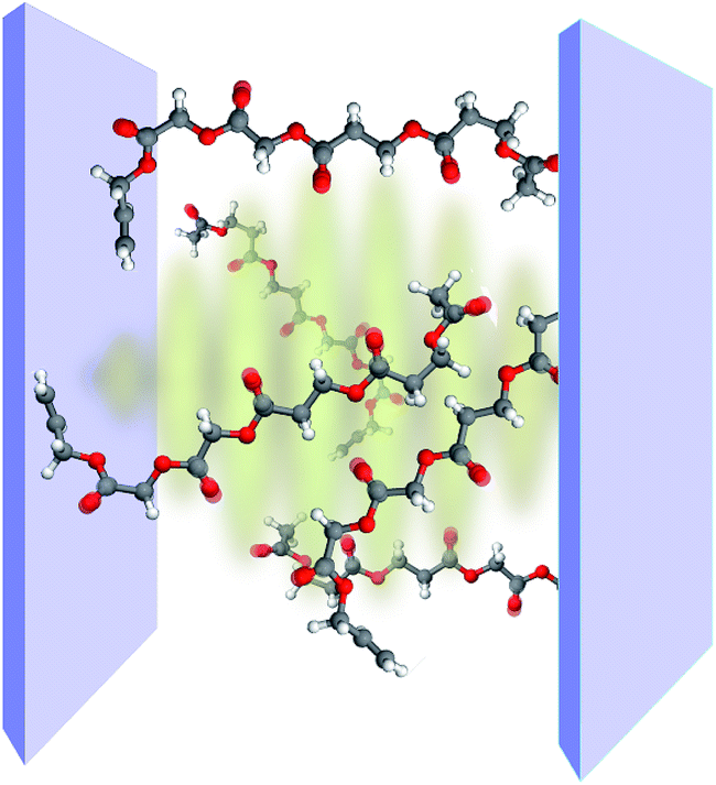
Modeling of Si / Cu nanoparticles based on a relationship between molecular mechanics and solid mechanics, an energy-equivalent model is used for the mechanical properties and nanomolecular structure of the sputtering layer of materials, macroscopic properties of nanoparticles such as melting point, boiling point and electrical conductivity. It is done through a sample that is large enough to be measured in normal laboratory conditions. When the melting point of a nanomolecule is measured, in fact, the behavior of a large number of nanoparticle molecules is examined, and this is not true for all materials; When the size of materials is reduced and reaches nanometer dimensions, completely different behavior and properties may be seen compared to the same material in large dimensions. The properties of nanomaterials and nanoparticles can depend on their size. This fact can be contradicted with the well-known fact that the properties of substances (solid, liquid and gas) are related only to the atoms and molecules that make up the substance and their bonding type or to the arrangement of the atoms. This is true in macro and micro dimensions. but everything is modified in nano dimensions, as a result of which the material properties may undergo fundamental changes.

Conclusion:
In nanoelectronics technology, special parameters and systems must be used to perform such processes. For example, in the metal marking process, it is inevitable to use copper metal instead of the common aluminum metal for internal connections between different practical parts. However, the rapid penetration of Cu atoms under Si during heat treatment leads to the formation of a copper silicide layer and ultimately causes the destruction of the electronic component.
Researcher and author: Dr. ( Afshin Rashid)
Specialized doctorate in nano-microelectronics