

_ Understanding ( Micro BGA ICs) or (Micro Ball Base)
Micro BGA or Micro Ball Base Internal Structure (Q_Micro BGA)
Researcher and Author: Dr. ( Afshin Rashid)

Note: The increase in the number of inputs and outputs in ICs has caused the dimensions of the IC to increase in order to both increase the number of pins and reduce the dimensions of the IC. Micro BGA technology is used. This chip model can be rebuilt or reballed.
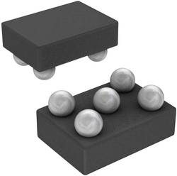
In this method, instead of the IC pins being around it, they are underneath the IC. The pins are soldered in the form of balls, which are soldered to the board after assembly.
How Micro BGA Works and Structure
There should be no holes under the base of this IC because the base will not be soldered properly. Via is used between the IC pads . Which is in two ways below.
Method 1: In this method , vias are placed between horizontal or vertical legs.

Second method: In this method, Vias are placed between four IC pads.
To avoid problems during IC assembly and to prevent short circuits between the via and the base, the vias must be printed in green. In the Protel software, the Tenting option must be selected in the Via specifications.

This chip model is a type of SMD IC. It is used in many electronic devices such as mobile phones and telecommunications equipment, computer motherboards and many other places in electronic boards. Because this IC does not have a base, which means it does not have a hard base like other DIP or SMD ICs, and its bases are made of tin and these bases are located exactly at the bottom of the IC; to replace it, we need a heater device; for this, we use an air heater, but for sensitive chips such as motherboards, an infrared heater can be used.
Micro BGA has a lower current to micro ball grid array (BGA) connection with less groove. Assembly services use mixed technologies such as chip and wire and use microelectronic assembly equipment in a clean room environment. The BGA uses a different method than that used in most common surface mount connections in the past. Other packages such as the quad flat package or QFP use the perimeter of the package for connections. This means that there is limited space for the pins to be close together and must be very small to provide the expected level of connection. The BGA uses the bottom of the package, where there is significant space for connections.
Researcher and Author: Dr. ( Afshin Rashid)
Specialized PhD in Nano-Microelectronics