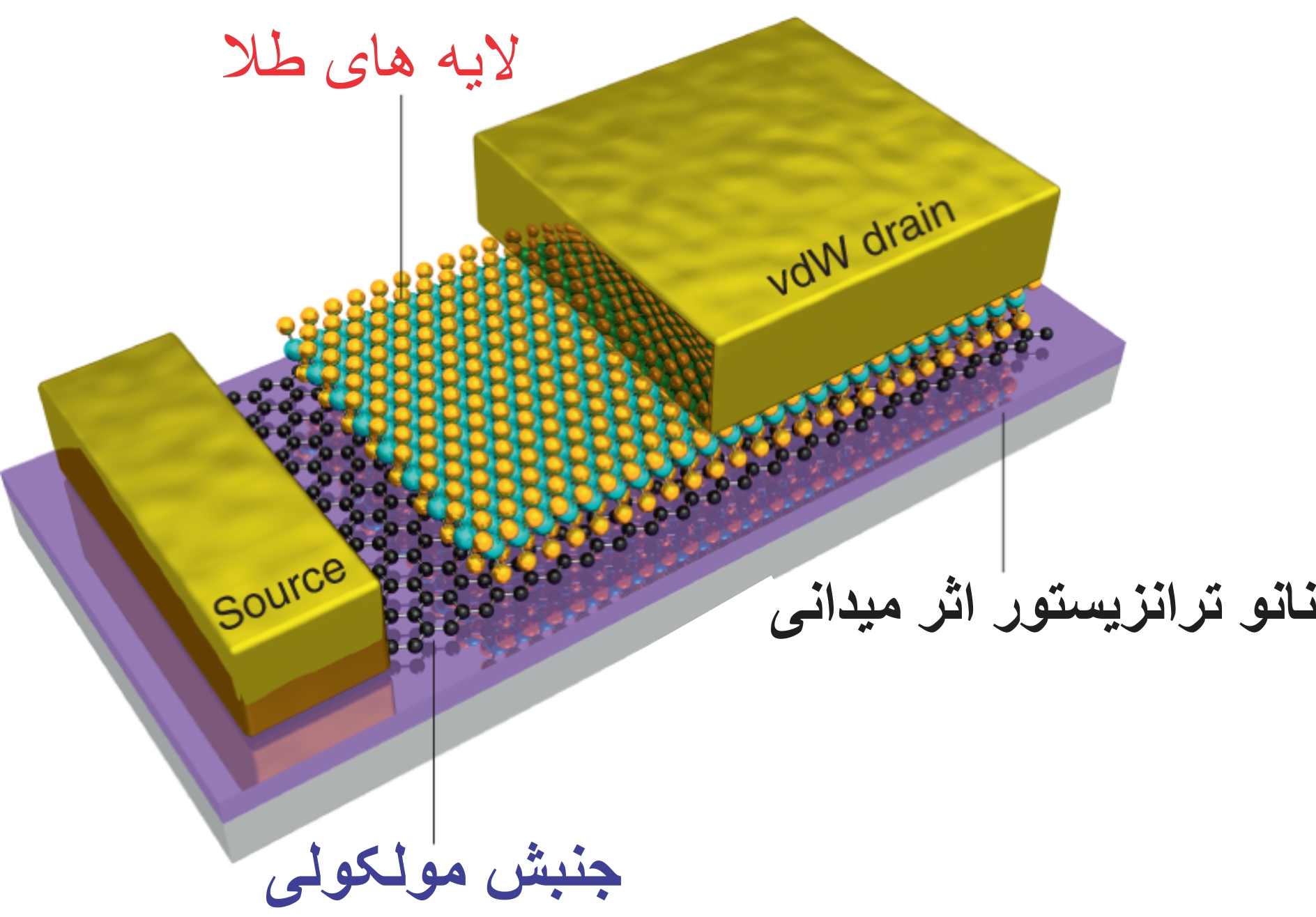
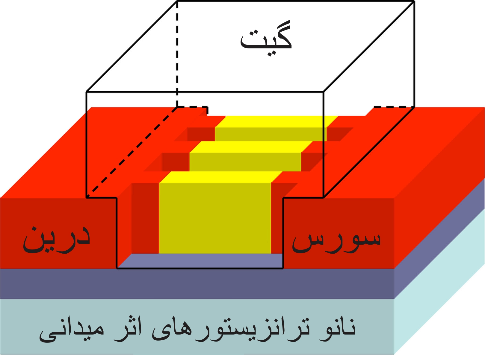
Field Effect Nano Transistors (Nano Teransistor Mosfet)
Field effect nano transistors and gold nano layers Nano Gold Layer
Researcher and author: Dr. ( Afshin Rashid)
Note: The interaction of gold nanoparticles with light is strongly determined by their environment, size and physical dimensions. The oscillating electric fields of a light beam emitted in the vicinity of a colloidal nanoparticle interfere with the free electrons and cause a coordinated oscillation of the electron charge that corresponds to the frequency of visible light. These resonant oscillations are known as surface plasmons. For small (30 nm) monodisperse gold nanoparticles, the phenomenon of surface plasmon resonance causes absorption of light in the blue-spectral part (~450 nm) while red light (~700 nm) is reflected.
Nano-microelectronics deals with new methods for making nano-transistors on a small scale, the dimensions of which are several tens of nanometers, which is derived from the science called nanotechnology. Unlike today's nanotransistors, which behave based on the movement of a mass of electrons in matter, new devices follow quantum mechanical phenomena at the nanoscale, in which the discrete nature of electrons cannot be ignored. By reducing all the horizontal and vertical dimensions of the transistor, the electric charge density in different areas of the nano-transistor increases, or in other words, the number of electric charges per unit area of the nano-transistor increases. This event has two negative consequences: First, with the increase in the electric charge density, the possibility of discharging the electric charge from the insulating areas of the transistor increases. And this event causes damage to the transistor and its failure. This event is similar to the discharge of excess electric charge between the cloud and the ground in the phenomenon of lightning, which causes the ionization of air molecules into negative and positive ions. Secondly , with the increase of the electric charge density, the electrons may leave the range of the radius of one atom and enter the range of the neighboring atom's radius under the influence of repulsive or abduction forces, which have now increased in value. This is called tunneling in quantum physics. Electron tunneling from one atom to the adjacent atom is a phenomenon that happens a lot between electrons in small dimensions. This phenomenon is the basis of the work of some electronic components and some nanoscopes. But in the nano transistor, the field effect of this phenomenon is not a useful phenomenon, because the electron tunneling from one atom to the adjacent atom may continue and cause an electric current.
In the nano transistor, the field effect of this electric current may be very small, but because it is unwanted and unanticipated, it acts as a leakage path for the electric current and changes the electrical behavior of the nano transistor.Gold is a soft and malleable metal with a bright and shiny yellow color that does not rust or darken in the vicinity of air and water. This metal can be found pure in nature in the form of grains or pieces among stones, minerals. Crystallized and alluvial deposits were found. The chemical symbol of this element, Au, is derived from its Latin name, aurum, which means "dawn's glow". Corrosion, distinctive color, non-reactivity with other elements, features that are seen in few other metals. One gram of this element can be hammered to the size of a sheet with an area of one square meter.
Conclusion :
The interaction of gold nanoparticles with light is strongly determined by their environment, size and physical dimensions. The oscillating electric fields of a light beam emitted in the vicinity of a colloidal nanoparticle interfere with the free electrons and cause a coordinated oscillation of the electron charge that corresponds to the frequency of visible light.
Researcher and author: Dr. ( Afshin Rashid)
Specialized doctorate in nano-microelectronics


