

DND self-organized electrical nanostructure and the effect of quantum confinement
Researcher and author: Dr. ( Afshin Rashid)

Note: Nanostructure electronic nanostructures are divided into four categories of zero-dimensional, one-dimensional, two-dimensional nanomaterials and three-dimensional bulk nanostructures based on their dimensions, which are on the nano scale. They can be produced bottom-up or bottom-up. Due to their very small size, nanostructures show special properties and sometimes different from other common materials in electrical conductivity.
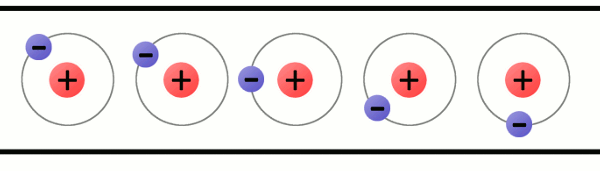
In general , nanostructures have three dimensions: length, width and height. If at least one of these dimensions is on the scale of nanotechnology (1-100 nanometers), it is called a nanostructured material. Nanostructures are divided according to how many dimensions they have on the scale of nanotechnology. One of these divisions is according to the number of free dimensions. Free dimension means a dimension that is not on the nanoscale and can have any value. There are energy structures (alignment or strip) of materials along each dimension of length, width and height. In other words, every three-dimensional object has three separate energy structures along its three dimensions, the result of which expresses the energy structure of the entire material.
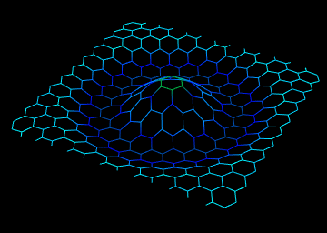
Dimensions of nanostructures that are on the nanoscale have so-called quantum confinement. For example, thin layers that have discrete energy levels in one dimension. Quantum limitation means that due to the limitation of nanoscale dimensions, the energy bands become discrete, and the greater the limitation (the smaller the dimensions), the greater the distance between the energy levels. Therefore, one of the main differences of different types of nanostructured materials is the number of continuous energy bands and discrete energy levels in three dimensions, which leads to many changes in their purity.
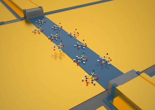
Electronic components can be produced by using nanoparticles under special conditions. This method is also suitable for producing memory and circuits with small dimensions. Nanoparticles are the most common elements in science and nanotechnology, and their interesting properties have made them widely used in chemical, medical and pharmaceutical, electronic and agricultural industries. According to the chemical composition, these particles are divided into metal, ceramic, polymer and semiconductor types. Chemical synthesis and solid state processes such as milling and vapor condensation are common methods for making nanoparticles. It is obvious to control the production process to reach nanoparticles with suitable properties, in this regard, to determine the characteristics of nanoparticles with microscopic and structural analysis methods and to determine the size and surface, etc., to examine the molecular connections that usually occur by sticking molecules to electrodes. Metals are created, they are able to reduce the dimensions of molecular tools. These connections have a high potential to have the same behavior and function as common electronic components. These molecular devices can be a good substitute or supplement for common technologies and create new capabilities in these technologies.

Conclusion:
Researcher and author: Dr. ( Afshin Rashid)
Specialized doctorate in nano-microelectronics