

Section (Self-organized electrical nanostructure)
DND self-organized electric nanostructure, a combination of (metal nanotube) and reaction with hydrogen and fluorine gas
Researcher and author: Dr. ( Afshin Rashid)
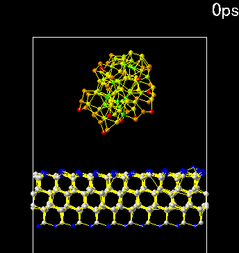
Note: In the electrical structure of hybridization (metal nanotube), the reaction with hydrogen and fluorine gas, by entering SP3, turns the hybridization structure of metal nanotube into a semiconductor.
These reactions sometimes destroy the walls of nanotubes and lead to the formation of amorphous carbon or graphite layered structures. By hydrogenation of single-walled nanotubes, the semiconducting nature of SWCNTs increases at room temperature. Strong plasma or reaction at high temperature causes the wall of metal nanotubes to be etched. that semiconductor SWCNTs are not damaged. Therefore, it is very important to control the reaction conditions. In nanotubes, the reaction with methane plasma removes metal SWCNTs without destroying semiconductor SWCNTs. In the method of using nanomolecular soft hydrogen plasma, in which hydrogen plasma is used to convert metal SWCNTs into semiconducting SWCNTs, and in this case, the walls of the nanotubes are not destroyed or etched. These reactions, which are carried out in the gas phase, cause in-situ and high-scale fabrication of TFTS and FETS with semiconductor nanotubes, which is very important for the commercialization of high-efficiency devices based on nanotubes. By choosing suitable reactive gases, this method can also be used for selective reactivity with semiconductor nanotubes. by reacting SWCNTs SO3 as under neutral gas in the presence of gas; Reactive gas inside the furnace at 400 C◦ temperature, semiconductor nanotubes are preferred with reactive gas . After that, the nanotube is heated to a temperature of 900°C to restore the metal nanotubes with structural defects. This process is a simple way to enrich the nanotube sample from metal nanotubes. The mass production of metal nanotubes can be done with a more precise control of the reaction conditions and finally increase the production scale of its uses, including conductive films and transparent electrodes.
In general, based on the reaction rate, selective covalent electrochemistry of metal nanotubes can be divided into two categories:
1- The first is that the metal nanotubes become a type of semiconductor, which causes the metal type to be turned off, and the other is the removal of the metal nanotubes. The first reaction is accompanied by the establishment of electrons and the loss of symmetry, and an energy gap in the Fermi level of the metal nanotubes. creates
2- The second reaction converts all conjugated systems into a series of smaller aromatic compounds by opening CC bonds in the nanotube structure . The final result of both cases is obtaining semiconductor nanotubes, which are suitable for making nanoelectronic equipment .

In selective covalent reactions, reactant concentration is always important. And when the concentration of the reactant is high , both types of nanotubes are affected by the reaction. For example, in the case of FETS, increasing the reactant concentration decreases the Off current, and as a result, the Off/On ratio increases to more than 105. On the other hand, the strong response reduces mobility, which is another important parameter for electronic equipment. Therefore, there should be a balance between the progress of the reaction and the final efficiency of the equipment.

Conclusion:
There are several drawbacks to covalent methods . First of all, most of the nanotubes are functionalized and as a result the electronic structure of SWCNTs is defective. Second, due to the strong reaction, it is difficult to purify the product from amorphous carbon. The most important thing is that there is no covalent reaction after which the (m,n) nanotube can be uniquely purified.
Researcher and author: Dr. ( Afshin Rashid)
Specialized doctorate in nano-microelectronics