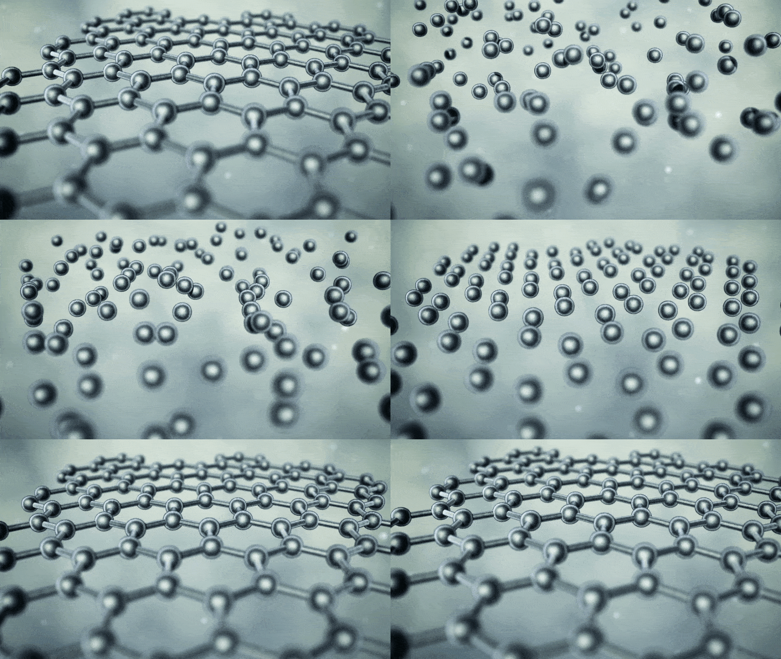
Section (Self-organized electrical nanostructure)
A final "summary of the topic" DND nanostructures or (self-organized electrical nanostructures)
Researcher and author: Dr. ( Afshin Rashid)

Note: In general, fundamental and controlled changes in the functional characteristics of DND nanostructures are used for their subsequent use in self-organization processes, in the preparation of nano-nano devices and electronic devices. The nanostructure is called DND (self-organized nanostructure).

Nanostructures refer to materials or structures that have at least one dimension between 1 and 100 nanometersThe importance of nanoscale is in changing the properties and characteristics of materials in these dimensions. Properties such as electrical conductivity, electromagnetic properties, etc. Starting to change the properties of the material by shrinking it depends above all on the type of material and the desired property. For example, by reducing the dimensions of a material, generally some of the electromagnetic properties of nano-molecular materials such as the conductivity of nano particles in materials are improved. This increase in strength does not happen only in the range of a few nanometers, and the strength of materials of several tens or even hundreds of nanometers may be much higher than the mass material of a large scale.

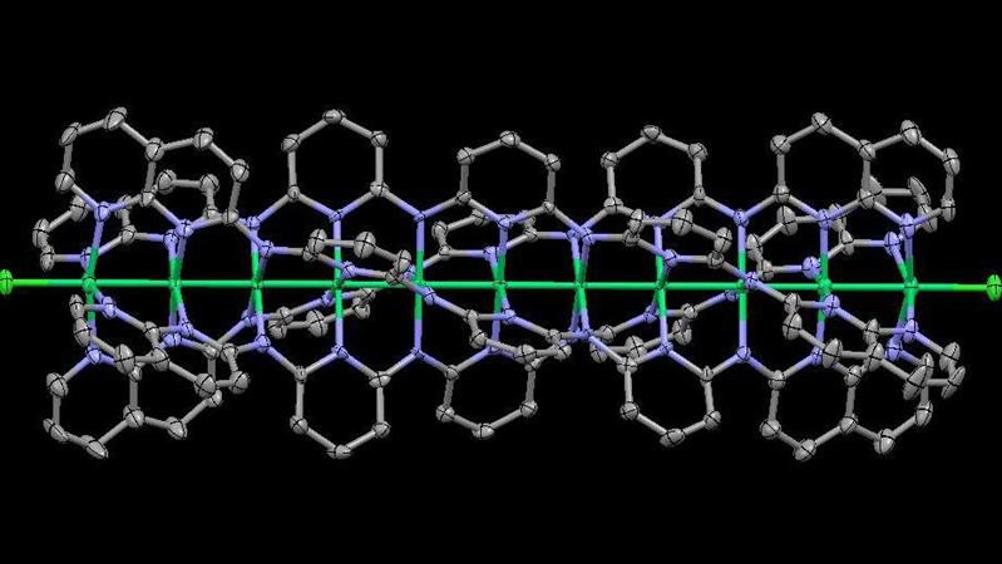
On the other hand, the change of some properties such as conductivity in nano-transistors and electromagnetic properties in nano-wires may occur in dimensions of only a few nanometers. Self-assembly (nanoparticles) in nanostructures is a spontaneous process by which nanomolecules/nanophases are transformed into organized functions. DND is an example of active wires. The structure of DND is well known and automatically this structure is created in the propagation of nanowires. The nanostructure of DND is an example of the proliferation of active wires, there is no problem to produce it like polymers, only its properties should be investigated to understand how it changes.

For this purpose, an example is mentioned:
In order to use DND to calculate the current in terms of voltage, a distance of 8 nm between two platinum electrodes is assumed, so by applying a voltage, the current can be calculated. The point that can be taken from the reaction is that the current diagram in terms of voltage is an asymmetric diagram, that is, the current is not allowed to pass for a voltage between 1 and 2 volts, for example, while it can pass for a current of 2 and 1 and this It means that DND can do the rectification.
Conclusion:
In general, fundamental and controlled changes in the functional characteristics of DND nanostructures are used for their subsequent use in self-organization processes, in the preparation of nano-nano devices and electronic devices. The nanostructure is called DND (self-organized nanostructure).
Researcher and author: Dr. ( Afshin Rashid)
Specialized doctorate in nano-microelectronics


