Nano electronics - Plasmonics to take advantage of significant advances in nano-scale electronics
Researcher and author: Dr. ( Afshin Rashid)
Note: In order to take advantage of significant advances in nanoscale electronics , there is an urgent need for high-performance, high-performance nanotechnologies that are compatible with frequent design changes. Common methods of maskless nano-lithography, such as plasmonic nano-lithography and probe scanning lithography, can provide desirable flexibility.
But it has been proven to be limited mainly due to their slow scanning capabilities. The technological properties of plasmonic lenses are such that they activate a point below 100 nm with approximately twice the intensity of the incident light. Used to achieve high speed scanning. By controlling the range according to the position of plasmonic nano-lithography on the surface of light resistance, an arbitrary high-speed nano-pattern with a spatial resolution of up to 80 nm is performed, such a low-cost and high-performance nano-fabrication method promises a new direction in production. Nano gives the next generation. This is a high-performance maskless nanolithography using plasmonic optical lenses at speeds of more than 20 miles per hour above an optical image. This research will also be applicable to other nanoproduction processes because it is the precise backbone of any nanoproduction process.
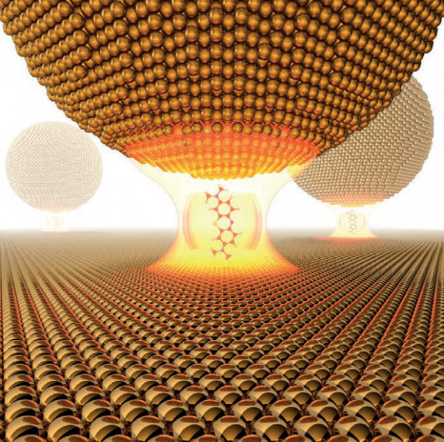
Nanoplasmonics is based on the interaction process between electromagnetic waves and conduction electrons in nanoscale metals. Analytically , it is the reason for the rapid drop in energy of electrons passing through metals. The free electrons become metal and it is called plasmon. These nanostructures are composed of metal and dielectric, the dimensions of which are below the excitation wavelength (the wavelength of the beam that excites the plasmonic waves). In the building of nanostructures (nanoplasmonics) The volume created by the electromagnetic field is localized, compressed and improved. Slight changes in the dielectric around the nanoparticle affect the intensification of surface plasmons, so that these changes are reflected in the amount of beam scattered, the absorbed beam, or the change in wavelength.
Conclusion :
In order to take advantage of significant advances in electronics science at the nanoscale , there is an urgent need for high-performance, high-performance nanotechnologies that are compatible with frequent design changes. Common methods of maskless nano-lithography, such as plasmonic nano-lithography and probe scanning lithography, can provide desirable flexibility.
Researcher and author: Dr. ( Afshin Rashid)
PhD in Nano-Microelectronics


