Application of plasmonic science in compression of nanoelectronic circuits and nanostructures
Researcher and author: Dr. ( Afshin Rashid)

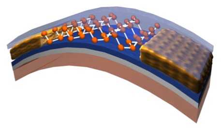
Note: With the technology approach to the aggregation of optical electronic circuits, fabrication problems and phenomena that helped prevent further compression of the structure, led to the use of plasmonic structures and plasmonic waves to be investigated and used. These nanostructures are composed of metal and dielectric, the dimensions of which are below the excitation wavelength (the wavelength of the beam that excites the plasmonic waves).
Plasmonics is based on the process of interaction between electromagnetic waves and conducting electrons in nanoscale metals. Analytically, it is the reason for the rapid decrease in the energy of electrons in the passage of metals, and concluded that this energy is used for the cumulative motion and oscillation of free electrons of metal, and called it plasmon. The reason for this naming was the similarity of these electron oscillations with the oscillations of the particles in the plasma environment. The term polariton is used to oscillate metal-bound electrons when paired with incident beam phonons. The name polariton was used for quasi-particles that were half-matter and half-photon, which is the coupled state between an elementary excitation beam photon and metal conduction electrons, and the term Plasmon Polariton to express the cause of a coupling between a photon and Is a plasmon.
The division of this nascent science into two domains of localized superficial plasmons and superficial polariton plasmons is briefly introduced each. In superficial superficial plasmons, nanoparticles are the basis of interactions, and their properties in stimulating this mode of plasmonic waves have been investigated. In surface plasmon polaritons, with the introduction of their working foundation, there is its field formulation and how these structures exceed the diffraction limit. Nanostructures have fundamental differences, both in terms of synthesis and production, as well as in terms of properties and applications. In general, the electrical, optical, magnetic, surface, etc. properties of these three structures are fundamentally different from each other, and of course their applications are also different. One-dimensional nanostructures can be used for electronic connections, while zero-dimensional and two-dimensional nanomaterials do not.The main basis of nanotechnology is the use of materials. Every material in space has three dimensions of length, width and height. If in materials at least one of these three dimensions is in the nanometer range, it is called a substance, a nanostructure.

Conclusion :
With the technology approach to the aggregation of optical electronic circuits, fabrication problems and phenomena that helped prevent further compression of the structure led to the use of plasmonic structures and plasmonic waves. These nanostructures are composed of metal and dielectric, the dimensions of which are below the excitation wavelength (the wavelength of the beam that excites the plasmonic waves).
Researcher and author: Dr. ( Afshin Rashid)
PhD in Nano-Microelectronics

