

Nanoelectronics and (nano-plasmonics)
Researcher and author: Dr. ( Afshin Rashid)
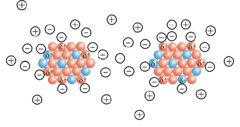
Note: In the building of nanostructures (nanoplasmonics) , the volume created by the electromagnetic field is localized, compressed and improved. Slight changes in the dielectric around the nanoparticle affect the intensification of surface plasmons, so that these changes are reflected in the amount of beam scattered, the absorbed beam, or the change in wavelength.
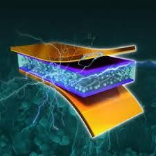
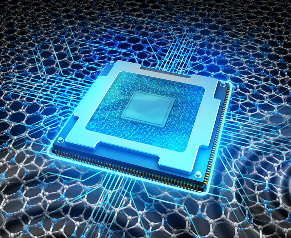
Nanostructure is defined as any structure with one or more dimensions and is measured in the nanometer scale range. Nanostructures are materials or structures that have at least one dimension between 1 and 100 nanometers . The importance of nanoscale in changing the properties and characteristics of materials in these dimensions. Properties such as electrical conductivity, electromagnetic properties and so on. The beginning of changing the properties of a material by shrinking it depends more than anything on the type of material and the desired property. For example, as the dimensions of a material shrink , some of the nanomolecular electromagnetic properties of materials, such as the conductivity of nanoparticles in materials, generally improve. This increase in strength does not occur only in the range of a few nanometers, and the strength of materials of several tens or even hundreds of nanometers may be very high. Be larger than large-scale bulk material. These changes can be measured using optical characteristics. The oscillations of surface electrons and the electric field around them indicate the intensification of localized surface plasmons.
For example, as the dimensions of a nanostructured material shrink , some of the mechanical properties of the material, such as strength, generally improve. This increase in strength does not occur only in the range of a few nanometers, and the strength of materials of several tens or even hundreds of nanometers may be much greater than that of large-scale mass material. On the other hand, changes in some properties, such as color and magnetic properties, may occur in dimensions of only a few nanometers. Nanoplasmonics is based on the interaction process between electromagnetic waves and conduction electrons in nanoscale metals. Analytically , it is the reason for the rapid drop in energy of electrons passing through metals. The free electrons become metal and it is called plasmon. These nanostructures are composed of metal and dielectric, the dimensions of which are below the excitation wavelength (the wavelength of the beam that excites the plasmonic waves).

Conclusion :
In the building of nanostructures (nanoplasmonics) , the volume created by the electromagnetic field is localized, compressed and improved. Slight changes in the dielectric around the nanoparticle affect the intensification of surface plasmons, so that these changes are reflected in the amount of beam scattered, the absorbed beam, or the change in wavelength.
Researcher and author: Dr. ( Afshin Rashid)
PhD in Nano-Microelectronics