

Silicone Wafers Silicone wafer A suitable support for growth and / or nanoparticles being installed (nanowires) (PhD in Nano-Microelectronics)
Researcher and author: Dr. ( Afshin Rashid)
Note: Silicone wafer is similar to glass, making it a good support for growth and / or nanoparticles being installed (nanowires). For nanoelectronic applications, due to the low background signal and highly polished surface, it is an ideal sample bed for small nanoscale particles.
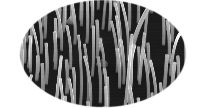
Silicon wafer substrates can be used for sample substrates, microfiber substrates, substrates for nanowires or biological substrates. Useful flat bed of silicone wafer particles Bonded with nanowires and for biological applications, Si (silicon wafer) has glass-like properties and can be used to mount or grow nanowire particles. It can be easily removed or used as a whole nanowire amplifier wafer. Silicon Nanowire Arrays or SiNWs are vertical arrays of silicon nanowires on a flat crystalline silicon wafer substrate. These nanowires are made by a catalytic oxidation and Si dissolution in the presence of metal catalyst nanoparticles - a self-organizing process commonly referred to as the metal-chemical amplified process with the help of Known as silicone wafers .
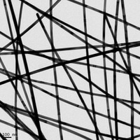
The processes of nanowire amplification on silicone wafer Silicone wafer make Si Nanowire arrays more reproducible and uniform, allowing the properties of nanowires to be adjusted. The nanowire amplification process always involves depositing a metal and bonding it in a solution containing hydrofluoric acid (HF) and an oxidizer. Silicon is produced only where metal nanoparticles touch the silicon, so electrochemical reactions with the mediation of nanoparticles. As the silicon is transported, the nanoparticles move into the resulting nanoparticles. Because silicon is only locally vaulted, this process can lead to properties with very high aspect ratios in nanowires.

Conclusion :
Silicone wafer For biological applications, silicone wafer is similar to glass, making it a suitable support for the growth and / or nanoparticles being installed in nanowires. For nanoelectronic applications, due to the low background signal and highly polished surface, it is an ideal sample bed for small nanoscale particles.
Researcher and author: Dr. ( Afshin Rashid)
PhD in Nano-Microelectronics