

SiNWs Silicon Nanowires (PhD in Nano-Microelectronics)
Researcher and author: Dr. ( Afshin Rashid)
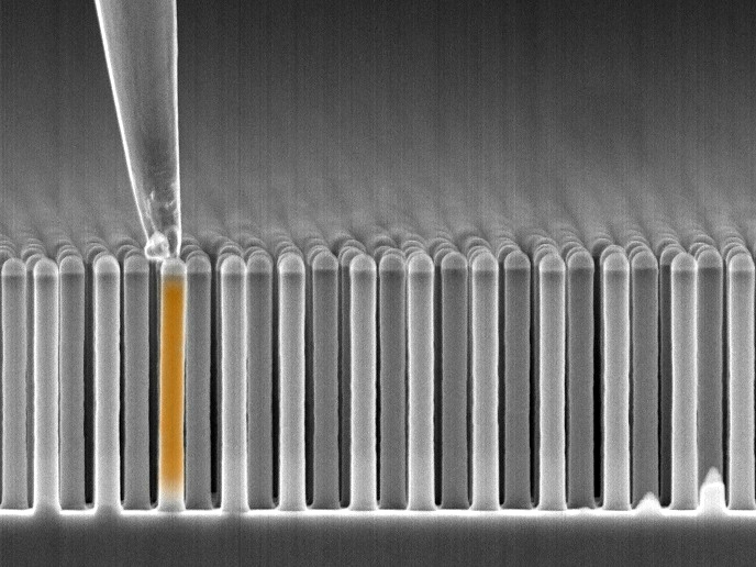
Note: Silicon nanowires are one of the best examples of semiconductor nanostructures that can be made in a single crystal with a diameter of 9 to 0 nanometers.
The advantages of SiNWs in the use and development of sensor platforms are due to the known properties of silicon and its optimum manufacturing processes. The physical properties of these nanowires include their electrical, photoelectric and mechanical properties. Nanowires ( SiNWs) have high mobility and surface-to-volume ratios, making them easy to control using a weak electric field. These nanostructures are made of one-dimensional nanowires with a diameter in the range of nanometers and a length of more than micrometers. The fabrication of nanowires from regular one-dimensional arrays has been done with the help of different physical and chemical methods. Methods such as electron beam or lithography, heavy ion irradiation, laser, chemical and electrochemical methods Like water heat, spontaneous aggregation methods used to make mold membranes can also be used .
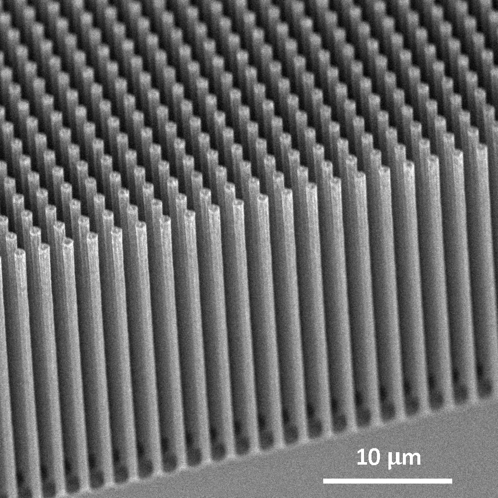
In the construction of one-dimensional nanostructures such as nanowires by electro-accumulation method, there are three general steps: first, the construction of a porous mold as a substrate and a suitable framework for the accumulation of nanowires, second, the growth of nanowires in the form of mold cavities and third, mold removal And the separation of nanowires. The properties of nanowires depend directly on the characteristics of the mold surface such as the size distribution of the holes, the density of the holes and the surface superiority of the nanopores. To control the properties of nanowires, the parameters that affect the formation and optimization of hole diameters and mold thickness must be considered. Magnetic nanowires such as cobalt, nickel, iron and alloys can be fabricated by electro-deposition and spontaneous aggregation on anodic aluminum oxide molds and the magnetic properties of cobalt nanowire arrays such as coercive force, electromagnetic saturation and magnetization. And The diameter of the nanowires depends. This property of nanowires can be easily controlled by changing the factors influencing the fabrication of the mold, such as the potential of the oxidation process and pH. Among the applications in chemical nano- sensors, nano-logic devices and other nano-electronic and nano-optical devices were mentioned.

Conclusion :
Silicon nanowires are one of the best examples of semiconductor nanostructures that can be made in single crystals with a diameter of 9 to 0 nanometers.