

Silicon nanowires are one of the best examples of semiconductor nanostructures (PhD in Nano-Microelectronics).
Researcher and author: Dr. ( Afshin Rashid)

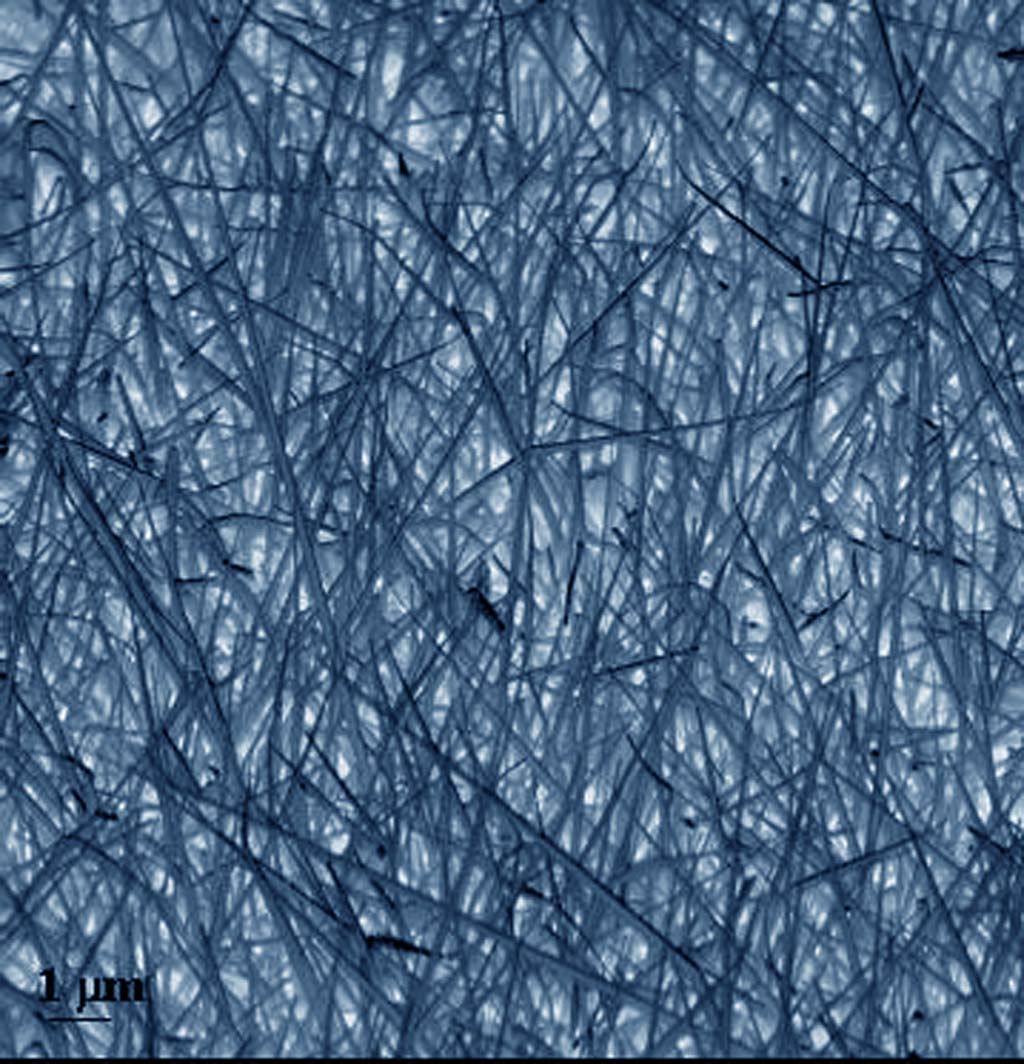
Note: Silicon nanowires are one of the best examples of semiconductor nanostructures that can be made in single crystals with a diameter of 9 to 0 nanometers.
Nanowires ( SiNWs) have high mobility and surface-to-volume ratios, making them easy to control using a weak electric field. The processes of nanowire amplification on silicone wafer Silicone wafer make Si Nanowire arrays more reproducible and uniform, allowing the properties of nanowires to be adjusted. The nanowire amplification process always involves depositing a metal and bonding it in a solution containing hydrofluoric acid (HF) and an oxidizer. Silicon is produced only where metal nanoparticles touch the silicon, so electrochemical reactions with the mediation of nanoparticles. As the silicon is transported, the nanoparticles move into the resulting nanoparticles. Because silicon is only locally vaulted, this process can lead to properties with very high aspect ratios in nanowires.
Nanowires are high-dimensional, large-area quasi-dielectric nanostructures in which radial strain uniformity allows unusable compounds of semiconductor materials. Enables countless applications of nanowires in electronics, optics and quantum technologies in general. Electromagnetic nature of nanoparticles In magnetic materials, the molecules and atoms that make them up have electromagnetic properties. Simply put, elements such as iron, cobalt, nickel and their alloys areabsorbedby the magnet . It is called magnetic material.The classification of electromagnetic materials is based on magnetic susceptibility (the ability of a material to become magnetic). Based on this, materials are classified into three groups: ferromagnetic, paramagnetic and diamagnetic. The result of bipolar moment in electromagnetic diamagnetic materials is zero, and in the presence of a magnetic field, dipole moment is induced in them; But the direction of these induced dipoles is opposite to the direction of the external magnetic field, which causes matter (diamagnetism) to be expelled from the magnetic field. By removing the external magnetic field, the magnetic properties of these materials do not remain. The magnetic susceptibility of these materials is negative and very low (about 6-10 -3-10). All gases (except oxygen) are water, silver, gold, copper, diamonds, graphite, bismuth, and many organic compounds ( diamagnets). Magnetic poles In paramagnetic matter, they do not have a definite and regular orientation; As a result, these materials have no magnetic properties. If they are placed inside a magnetic field, they are aligned along the lines of the magnetic field. With the removal of the magnetic field , the magnetic dipoles quickly return to their previous state in the absence of the field. In this way, paramagnetic materials acquire strong magnetic properties in nano-electromagnetic fields.

Conclusion :
Silicon nanowires are one of the best examples of semiconductor nanostructures that can be made into single crystals with a diameter of 9 to 0 nanometers.
Researcher and author: Dr. ( Afshin Rashid)
PhD in Nano-Microelectronics