

_ Department (Nano and Micro Electromechanical MEMS )
(Nano and Micro Electro -Mechanical MEMS ) and the creation of new devices and tools in nanoelectronics
Researcher and author: Dr. ( Afshin Rashid)
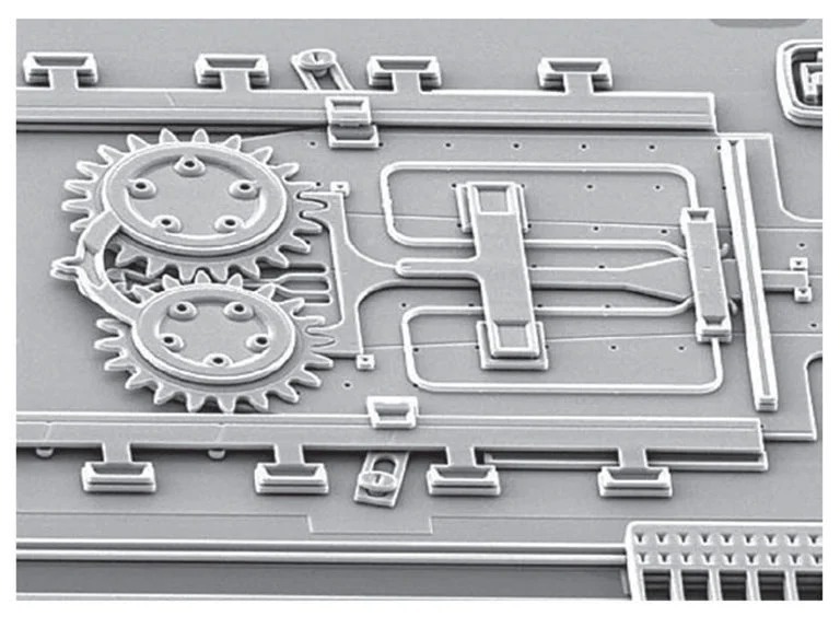
Note: To replicate and fabricate nano and micro electro -mechanical MEMS systems , we use a set of techniques using a nanoparticle solution, which we deposit in a very thin layer on the desired substrate and use as an intermediate layer during the nano-patterning process.
For the propagation and fabrication of (nano and microelectromechanical MEMS) systems , due to the interaction between nanoparticles, they can organize themselves and form a thin layer that creates holes between them, this technique was initially called natural lithography . Due to the integral nature of colloidal particles and their hydrophilic property, they form a colloidal crystal with ordered pores through which the materials of interest penetrate and deposit on the substrate. For example, polystyrene latex nanospheres can be used. The materials deposited on the nanoparticles disappear after immersing the sample in a suitable solvent and sonication. This process in the propagation and fabrication of (nano and microelectromechanical MEMS) systems is similar to a removal process . The advantages of this technique include large patterns, simplicity, good resolution and the ability to be combined with other techniques for the propagation and fabrication of (nano and microelectromechanical MEMS)systems . On the other hand, this technique poses problems due to the limited shapes available for patterned functional materials, the range arrangement of nanopatterns, and the presence of point defects.
In general, if two techniques for the fabrication of nano- and micro-electromechanical MEMS systems can complement each other in terms of resolution or pattern area, it makes sense to combine them into a single device. This approach has been used to fabricate single-electron transistors, integrating direct laser writing for large-area exposure and thermal probe lithography for high-resolution patterns . The fabrication of nano- and micro- electromechanical MEMSsystems is achieved using a nanolithographic resist layer , in a process that is designed to be mix-and-match. This concept typically involves the sequential use of a large-area nano- and micro -electromechanical MEMSsystem fabrication technique for non-critical dimension patterns and a high-resolution lithography technique for patterning the smallest dimensions, with appropriate protocols for the alignment of the nano- and micro-electromechanical MEMS systems . For the propagation and fabrication of (nano- and micro-electro -mechanical MEMS)systems, it has also been used to perform sequential exposure of chemical resists enhanced by photolithography and electron beam lithography. For the propagation and fabrication of (nano- and micro- electro-mechanical MEMS) systems , it is used top-down lithography and bottom-up self-organization of two polymers to produce high-resolution nanopatterns over large areas . Typically, the self-organization of the block copolymer is randomly oriented and lacks long-range order , but the previous top-down pattern provides a substrate for the propagation and fabrication of (nano- and micro-electro -mechanical MEMS)systems . , (nano- and micro- electro-mechanical MEMS)systems A substrate promotes the preferential growth of semiconductor materials in the irradiated areas, which can be used to fabricate ordered arrays of semiconductor dots.

Conclusion:
To replicate and fabricate nano- and micro -electromechanical systems (MEMS ) , we use a set of techniques using a solution of nanoparticles, which we deposit in a very thin layer on the desired substrate and use as an intermediate layer during the nano-patterning process.
Researcher and author: Dr. ( Afshin Rashid)
Specialized PhD in Nano-Microelectronics