

_ Department (Nano and Micro Electromechanical MEMS )
Examining the principles of manufacturing and placing a MEMS ( nano- electro -mechanical) system
Researcher and author: Dr. ( Afshin Rashid)
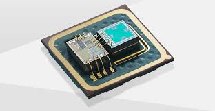
Note: MEMS are integrated into moving microstructures (with electromechanical components), sensors, actuators, radiant energy devices, and microelectronics. These MEMS can be fabricated for use in various microfabrication technologies such as micromachines.
The fundamental technology in the fabrication of MEMS, CMOS and biCOMS (for the fabrication of ICs) and micromachines (for the generation of motion and radiation and the emission of energy to micron-scale devices and structures). One of the main goals is to integrate microelectronics with electromechanical micromachine devices and structures to produce integrated and high-performance MEMS . To ensure high performance, workability, reliability and manufacturability, CMOS-based bulk fabrication processes are well developed and need to be refined and enhanced.
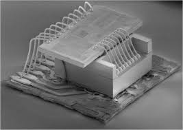
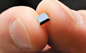
Bulk body micromachining in MEMS components
Micromachining of the surface and the bulk (BULK) as well as high-aspect ratio (LIGA-like and LIGA) technologies are the most developed fabrication methods. Silicon is the primary substrate material used in the microelectronics industry. A crystal mold ( a solid cylinder 300 mm in diameter and 100 mm long) of very high purity silicon is crystallized, cut to the desired thickness, and then polished using mechanical and chemical polishing technologies . The properties of the electromagnetic and mechanical plates are the direction and location of crystal crystallization and its expected impurities. Depending on the silicon substrate, CMOS and biCMOS processes are used to produce ICs, and bulk and surface micromachining (as well as high-aspect ratio (LIGA-like) and LIGA-like technologies) are the most developed fabrication methods. Silicon is the primary substrate material used in the microelectronics industry. A crystal mold ( a solid cylinder 300 mm in diameter and 100 mm long) of very high purity silicon is crystallized, cut to the desired thickness, and then polished using mechanical and chemical polishing technologies . The properties of the electromagnetic and mechanical plates are determined by the crystal orientation and the expected impurities. Depending on the silicon substrate, CMOS and biCMOS processes are used to produce ICs and the processes are classified as: n-well, p -well, or well-twin. The main steps are: diffusion, oxidation , polysilicon gate formation , photolithography, gate formations , masking, etching, metallization, wire bonding , etc. The following are the main and basic processes and steps in MEMS manufacturing.
Processes are classified as:
N well-n source, (p-source) (well-p) (or well-twin source) (the main steps are: diffusion, (oxidation)
(oxidation, polysilicon gate formations, photolithography, photoetching)
Masking, etching, metallization, wire bonding, etc. Below we list the major and basic processes and steps of MEMS manufacturing.
Step 1 ( Grow Silicon Dioxide):
(Silicon dioxide is crystallized thermally on a silicon substrate. For example, crystallization can be carried out in a steam-filled atmosphere at 1000° C for one hour. Silicon surfaces are covered with a layer of silicon dioxide 0.5 to 1 micron in diameter (the thickness of the thermal oxide is limited to a few microns by the diffusion of water vapor along the silicon oxide). Silicon dioxide can be deposited without changing the underlying surface, but this process is so slow that it minimizes the pressure of the thin membrane. Silicon nitride may also be deposited, and its thickness is limited to 4 to 5 micron.
Stage 2: (Photoresist)
Photoresist: A photoresist (a photosensitive material) is applied to the surface of silicon dioxide. This can be done by spinning the photoresist coating suspended in a solvent. The result after spinning and removing the solvent is a photoresist with a thickness of 0.2 to 2 microns. The photoresist is then fully cured and soft enough to remove the solvents from it .

Stage 3 ( Photolithography Exposure, and Development )
A photoresist is like a photoetching mask ( photomask) exposed to ultraviolet light. This photomask blocks the path of light and defines a pattern to ensure the desired surface mapping . Photomasks are typically made using fused silica and optical transparency that is subjected to wavelength, width, and thermal expansion to an effective limit . A patterned opaque layer is deposited on a glass or (quartz) surface ( usually a layer of chromium hundreds of angstroms thick). A photomask is produced based on the required shape of the silicon polyshell. The surface mapping is determined by the mask. The photoresist is then created. In a positive photoresist, light reduces the molecular weight of the photoresist, and the photoresist generator selectively removes the lowest molecular weight materials.
Step 4 (Etch Silicon Dioxide):
The silicon dioxide is etched away . The remaining photoresist is used as a hard mask that protects the silicon dioxide section. The photoresist is removed by wet etching ( hydrofluoric acid, sulfuric acid, and hydrogen peroxide) or dry etching (using oxygen plasma). The result is a thin film of silicon dioxide on the silicon substrate .
Step 5 (Polysilicon Deposit:
(A thin film of polysilicon is deposited on silicon dioxide. For example, polysilicon can be deposited in an LPCVD system at 600°C in a confined space of silane (SiH4) . The deposition rate under normal conditions is 65 to 80 Angstroms per minute (Almin), which minimizes internal stress and prevents warping and folding . (The polysilicon thin film must be stress-free or have a tensile internal stress.) The thickness of the thin film is greater than ((4)) microns.
Conclusion on the method of manufacturing and replicating the MEMS system

With the work done in the field of NEMS, MEMS, today the industry has moved more towards micro and nanoelectronics. Therefore, research work in this field seems to be mandatory, which will result in the achievement of superior science and technology of the century. Among the future works that should be done in this field is the optimal design of MEMS and the achievement of its modified forms for work in other sciences.
Researcher and author: Dr. ( Afshin Rashid)
Specialized PhD in Nano-Microelectronics