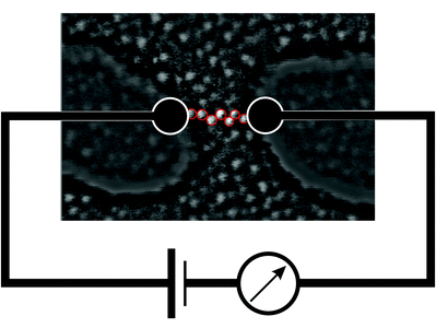
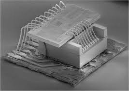
_ Section of the simulation process in (electrical nanoparticles)
Analysis and investigation of the simulation of electrical nanoparticles in manufacturing (nano-transistors-nano-regulators)
Researcher and author: Dr. ( Afshin Rashid)
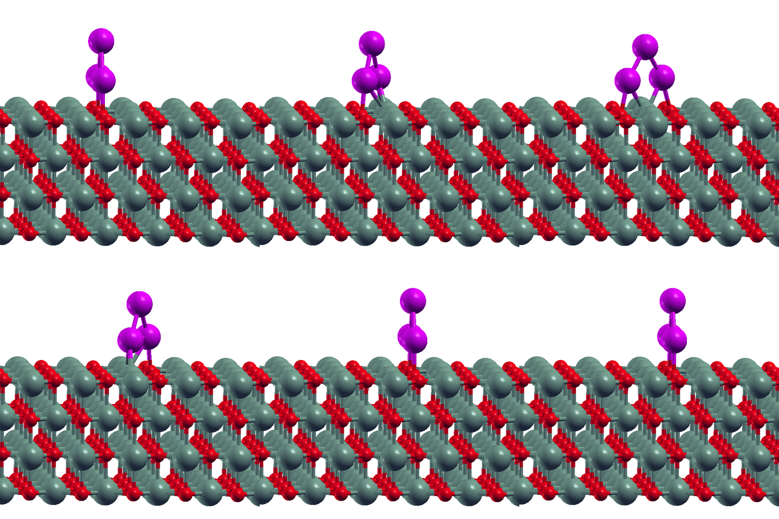
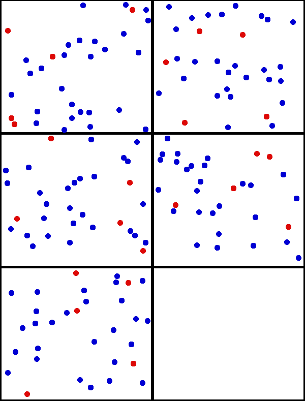
Note: Nano MOSFET) and Double Gate MOSFET (DG MOSFET) transistors simulated with DGMOSFET structure have lower Ioff than SOI structure. Ion/Ioff ratio in DG structure is higher than SOI structure. The effect of reducing the drain-induced potential barrier (DIBL) in SOI MOSFET is more intense than that of DG MOSFET structure. DG has higher mobility than SOI structure.
Nanoscale MOS transistors are used in computers with very compact electronic integrated circuits. In order to further miniaturize circuit components to the nanoscale, perhaps even the molecular scale, researchers have proposed several alternatives to the transistor in the ultra-compact circuit. These nanoscale electronic devices act as both switches and amplifiers, similar to current transistors. But, unlike today's field-effect transistors, which operate based on the movement of electron masses in bulk matter, the new device takes advantage of quantum mechanical phenomena that occur at the nanoscale.
At first, the usual transistors and their limitations and the problems of their miniaturization are discussed, and to solve this problem, solid state transistors that take advantage of quantum effects at the nano scale, and among them, the resonant tunneling transistor sample is used. Electronic computers have become much more powerful than in the past and transistors have gradually become smaller. However, reducing the size of current field effect transistors will be impossible in the near future due to the effects of quantum mechanics and the limitations of manufacturing techniques. In the coming years, as the mass production of transistors will decrease from their current size to below 100 nm, it will become difficult and expensive to manufacture the device. In addition, they can no longer perform well as ultra-compact integrated circuits. To overcome this problem, there are basically two main classes of nanoelectronic switches that are also used as amplifiers.
Conclusion:
Nano MOSFET) and Double Gate MOSFET (DG MOSFET) transistors simulated with DGMOSFET structure have lower Ioff than SOI structure. Ion/Ioff ratio in DG structure is higher than SOI structure. The effect of reducing the drain-induced potential barrier (DIBL) in SOI MOSFET is more intense than that of DG MOSFET structure. DG has higher mobility than SOI structure.
Researcher and author: Dr. ( Afshin Rashid)
Specialized doctorate in nano-microelectronics


