

Section _ Construction and formation of field effect transistors (Mosfet)
Understanding and examining how field effect transistors (MOSFETs) are formed
Researcher and author: Dr. ( Afshin Rashid)
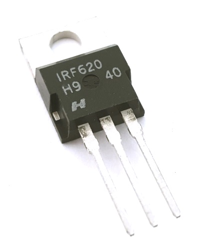
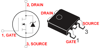
Note: A metal-oxide-semiconductor field-effect transistor (MOSFET, MOS-FET, or MOS FET) is a field-effect transistor (FET with an insulated gate) in which the conduction voltage of the device is determined. It is used to switch or amplify signals. The ability to change the conductivity with the amount of voltage applied can be used to amplify or switch electronic signals in a circuit. MOSFETs are now more common in digital and analog circuits than bipolar junction transistors (BJTs). A MOSFET transistor consists of three terminals: Gate / Source / Drain.
MOSFETs are by far the most common transistor in digital circuits, as hundreds of thousands or millions of them may be incorporated into a memory chip or microprocessor. Because they can be made from either p-type or n-type semiconductors, complementary pairs of MOS transistors can be used to make very low-power switching circuits in CMOS logic. A MOSFET has three terminals, the drain D, the source S, and the gate G, with the gate terminal controlling the current flowing from the drain to the source. MOSFETs come in two types: N-channel and P-channel. In an N-channel FET, current flows from the drain to the source when the gate is positive relative to the source. MOSFETs are usually very sensitive and can even be excited by static electricity on the body. For this reason, they are very sensitive to noise. Another type of field effect transistor is MOSFET - Metal Oxide Semiconductor Field Effect Transistor. One of the most important advantages of MOSFETs is their lower noise in the circuit.MOSFETs are also widely used in the construction of transmitters and telecommunications and radar systems.

MOSFETs are very useful in amplifiers because they have an almost infinite input impedance, which allows the amplifier to capture almost all input signals. The main advantage is that they require almost no input current to control the load current, compared to bipolar transistors. A field effect transistor (MOSFET) is considered to have three terminals called gate, drain, and source. In this transistor, the gate (control terminal) does not draw any current, and as the name suggests, the current through the FET is controlled only by applying a voltage and creating an electric field within the semiconductor. Therefore, when the gate is considered as the input of this transistor, it does not have any loading effect on its previous stages in the circuit, and the transistor in this case has a very high input impedance. The main difference between MOSFETs and other transistors is that the gate of MOSFET transistors is separated from the channel by a layer of silicon oxide (SiO 2 ).
Different in function and structure from the bipolar junction transistor, the MOSFET is made by placing an insulating layer on the surface of the semiconductor and then placing a metal gate electrode in it. This is a crystalline silicon semiconductor and a layer of silicon dioxide is used for insulation.
Researcher and author: Dr. ( Afshin Rashid)
Specialized PhD in Nano-Microelectronics