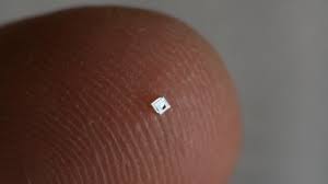
The most important parameters affecting the optimal dimensions of Nano Chips (based on PhD in Nano _ Microelectronics)
Researcher and author: Dr. ( Afshin Rashid)
Note: Most chips and nanochips are made of silicon. By applying the appropriate voltage (threshold voltage) to the silicon solution, the repulsive force overcomes the surface tension of the silicon and a jet is formed. By evaporating the solvent from the jet, the liquid-to-solid phase changes and nanoparticles of the chips are formed.
Many parameters affect the characteristics of nanostructures produced by this method, the most important parameters are the distance between the needle and the collector, the applied voltage, the flow rate and the concentration of the silicon solution; By changing these parameters, the optimal dimensions of nanochips can be achieved. The diameter of nanostructures is linearly related to the flow rate and distance and non-linearly related to the potential and concentration of silicon solution in the production of nanochips and nanotransistors. As the distance and electrical potential increase, the diameter of the nanostructures decreases and increases with increasing current rate and electrical potential.
In the production of nanoparticles and nanotransistors, the electric field reaches a critical value or threshold when the repulsive force overcomes the surface tension. First, the jet moves in a linear pattern, then slowly moves away from the linear pattern, forming a complex shape along the path to the collector. The structure and structure of the production of nano-chips and nano-transistors and the length of the jet are proportional to the applied voltage. The structure of the Taylor nano-cone changes from convex to concave by changing the field strength and consequently (jet charge density). The shrinkage of components in microelectronic systems and circuits has led to significant growth in the industry in recent years. The growth rate of this industry is such that as the components become smaller, the number of transistors per unit area of each semiconductor chip and nanocip has increased.Reducing the dimensions of these components can reduce the consumption of raw materials and energy, reduce the cost of these components and increase their speed and efficiency . Therefore, the construction and development of electronic tools with smaller dimensions and higher speed and efficiency has become more important day by day. Lithography is one of the most common methods for making electronic circuits. With the help of this method, structures with precision and dimensions of 01 nanometers can be made. Finding techniques that can be used to industrially produce these components (nanochips and microchips).
Conclusion :
Most chips and nanochips are made of silicon. By applying the appropriate voltage (threshold voltage) to the silicon solution, the repulsive force overcomes the surface tension of the silicon and a jet is formed. By evaporating the solvent from the jet, the liquid-to-solid phase changes and nanoparticles of the chips are formed.
Author: Dr. ( Afshin Rashid)


