Plasmonic nano-lithography in contact mode (less than 2 nanometers) in the manufacture of nanoelectronic devices and tools (PhD in nano-microelectronics)
Researcher and author: Dr. ( Afshin Rashid)
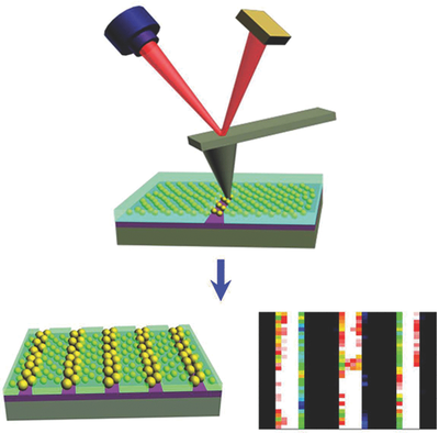
Note: For contact plasma nano-lithography, an optical probe that has a nano-diaphragm with high transmissibility and width in a metal film. To protect the diaphragm from contamination and abrasion, the optical probe is filled with a dielectric material in the hole and covered with a dielectric protective layer whose thickness is adjusted by the gap between the probe and the substrate.
The electric field distribution in the entangled diaphragm structure in an aluminum film at a wavelength of less than 2 nm with a direct-axis polarized impact beam is calculated using nano-electron plasmonic contact lithography in the manufacture of nanoelectronic devices and tools. Realistic simulation of the modeling process on the fabrication resistance of nanoelectronic devices and tools is the wave intensity of the silicon glass dielectric media impact plate , which is transparently and easily coated with plasma nanoparticle chemical vapor deposition during the wavelength.
Using a local electric field generated by a metal nano-diaphragm, plasmonic lithography can achieve a resolution less than diffraction. It is well known that the pattern recorded with a nano-diaphragm is quite different from the pattern created by an electric field in a conventional lithographic system, because the electric field around the diaphragm in the direction of the diaphragm hole in the metal film decays strongly. According to plasmonic lithography modeling, there is an exchange between pattern sharpness and depth as the pattern profile increases with increasing incident dose. We draw the width and depth of the line pattern recorded in several different exposure doses. We also calculated the width and depth using a plasmonic lithography model. The width and depth of the experimental line patterns qualitatively follow the calculated curves, although there are small differences. Small defects in the fabrication of metal nano-diaphragms may reduce the transmission and result in a slightly larger point size with less depth.
Conclusion :
For contact plasmon nano-lithography, an optical probe with a nano-aperture with high transmittance and width in a metal film. To protect the diaphragm from contamination and wear, the optical probe is filled with a dielectric material in the hole and covered with a dielectric protective layer whose thickness is adjusted by the gap between the probe and the substrate.
Researcher and author: Dr. ( Afshin Rashid)
PhD in Nano-Microelectronics


