Section _ reproduction and production of nanowires
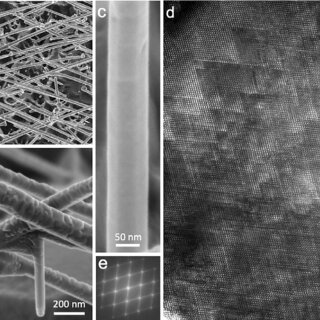
Morphology and phases of nanowires/nanotubes by transmission electron microscope (TEM) and X-ray diffraction (XRD) respectively.
Researcher and author: Dr. ( Afshin Rashid)
_e2f.gif)
Note: Cobalt nanowires technology in the approximate dimensions of 1 to 100 nm, where only one phenomenon of its kind offers descriptive applications, is in the capacity of matter.
Cobalt nanowires exhibit electromagnetic absorbing behavior at medium temperature and when the magnetic field is applied perpendicular to the nanowires, these nanoelectronic devices have a larger coercive field compared to when the electromagnetic field is parallel to the nanowires. Cobalt wires are formed. Nanotechnology encompasses science, engineering and non-scale technology, imaging, measurement, design and manipulation of materials at this length scale. Due to nanotechnology, the speed of computers has increased compared to the past and the value of calculations has decreased. In the immersion method, the nanowires have enough time to transfer from the particles of the nanowires to the holes; The step of forming uniform nanoparticles is done slowly and finally uniform nanowires are formed. Structural investigation with FESEM in the immersion method of uniform nanowires in all pores and in a wide area in nanowire particles. The simple answer to this question is any particle less than 100 nanometers. But as the scale of 1-100 nm determines the size range of a nanoparticle. In order to prevent particle contact, a cluster of atoms may be removed below 1 nm, but the electron movement in nanoparticles has to particles <1 nm. Because particles are three-dimensional.
Cobalt nanowires with a diameter of about 93 nm are made using electroplating technique on the aluminum mold of nanowires by galvanostatic deposition method. Aluminum mold is made through multi-stage monodizing of pure aluminum sheet. Fabrication of arrays of vertical cobalt nanowires aligned on flat surfaces and field emission (FE) by using them as electron cathodes. These arrays are made by electrodeposition in the form of nanoparticles on Au substrates. Ti/Si are obtained at very low temperature (<100°C). After pattern removal, the arrays consist of structurally upright nanowires with high aspect ratios, uniform dimensions, and predetermined densities. Electron field emission measurements of metallic properties and propagation of cobalt nanowires. In the reproduction of cobalt oxide nanotubes, cobalt nanowires embedded in alumina pattern are synthesized in air.

The morphology and phases of nanowires/nanotubes are investigated by transmission electron microscope (TEM) and X-ray diffraction (XRD), respectively. The electronic reaction of cobalt nanowires between the oxidation and evaporation of cobalt nanocrystals plays an important role in the formation of such an electronic nanostructure.
Conclusion:
The technology of cobalt nanowires in the approximate dimensions of 1 to 100 nm, where only one phenomenon of its kind offers descriptive applications, is in the capacity of matter.
Researcher and author: Dr. ( Afshin Rashid)
Specialized doctorate in nano-microelectronics


