

Section _ reproduction and production of nanowires
Investigating the production and reproduction of nanowires using nano-electron lithography
Researcher and author: Dr. ( Afshin Rashid)
_iwu.gif)
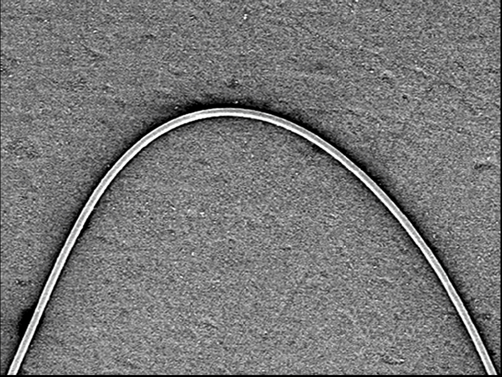
Note: Electron beam nanolithography is usually performed in a special environment or in equipment designed for this purpose. In both cases, a precisely focused electron beam is sequentially scanned along the sample to reveal the resistance.
The electron beam nanolithography process is inherently slow compared to other methods because the electron beam requires a limited amount of time at each exposure point. It is rare to see multiple exposures to the same specimen. Some developments are underway for multi-electron beam exposure . In contrast to long exposure times, very high resolution (below 100 nm) is typically achieved by electron beam nanolithography, and with a little optimization and the right equipment, it reaches the 10 nm range, as is the case in electron beam nanolithography. Thus, positive and negative resists are available in electron beam nanolithography , as well as the ability to perform lift-off processes that save the etching step.
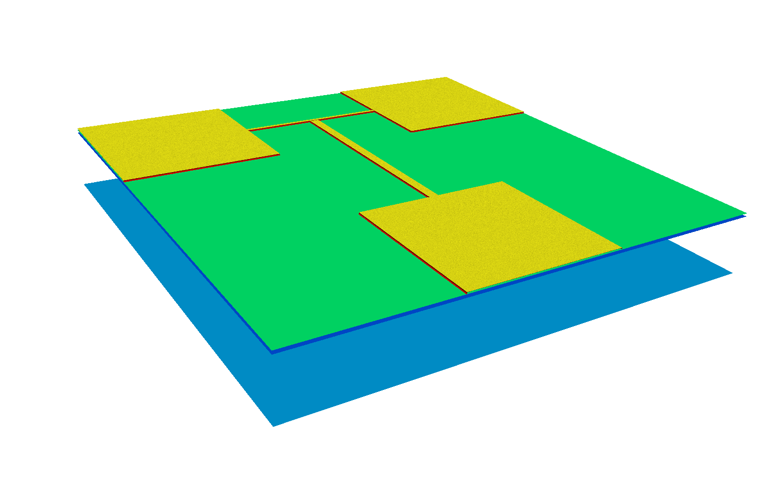
Electron beam nanolithography is a suitable technique for laboratory research and prototyping, given that throughput is not an important issue and a very good solution is obtained. Similarly to electron beam nanolithography , the nano process relies on changing the solubility of the resist after exposure. However, in electron beam nanolithography, an electron-sensitive resistor should be used instead of a photodetector.
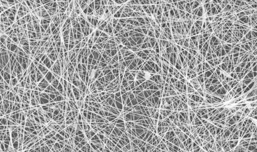
The processes of nanowire propagation on silicon wafers make the Si Nanowire arrays more reproducible and uniform, and allow the properties of the nanowires to be tuned. The propagation process of nanowires always involves the deposition of a metal and bonding in a solution containing hydrofluoric acid (HF) and an oxidant. Silicon is produced only where metal nanoparticles touch silicon, as a result of electrochemical reactions with the help of nanoparticles, as silicon is carried, the nanoparticles move into the resulting nanoparticles. Since silicon is only locally doped, this process can lead to very high aspect ratio features in nanowires. A useful flat base of silicon wafer particles linked with nanowires and for biological applications, Si (silicon wafer) has properties similar to glass and can be used to mount or grow nanowire particles. It can be easily wiped off or used as a whole wafer for the propagation of nanowires. Silicon nanowire arrays or SiNWs are vertical arrays of silicon nanowires on a flat crystalline silicon wafer substrate. These nanowires are made by a catalytic oxidation and dissolution of Si in the presence of metal catalyst nanoparticles - a self-organized process commonly known as silicon wafer- assisted metal-chemical enhanced process.

Conclusion:
Electron beam nanolithography is usually performed in a special environment or in equipment designed for this purpose. In both cases, a precisely focused electron beam is sequentially scanned along the sample to reveal the resistance.
Researcher and author: Dr. ( Afshin Rashid)
Specialized doctorate in nano-microelectronics