

Duplicate nano wires Oligofenylene Vanillin using nano-lithography and focused ion beam or (FIB) (100 nm, 10 nm range _) (_ PhD in nanotechnology microelectronics)
Researcher and author: Dr. ( Afshin Rashid)
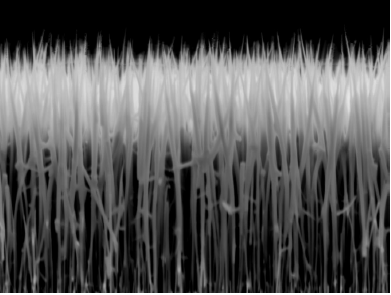

Note: The physical properties of Oligofenylene vanillin nanowires include their electrical, photoelectric and mechanical properties.
Nanowires ( SiNWs) have high mobility and surface-to-volume ratios, making them easy to control using a weak electric field. These nanostructures are made of one-dimensional nanowires with a diameter in the range of nanometers and a length of more than micrometers. In making nanowires from regular one-dimensional arrays with the help of different physical and chemical methods. Methods such as electron beam or lithography, heavy ion irradiation, laser, chemical and electrochemical methods such as water heat, and spontaneous aggregation methods used to make mold membranes can also be used . In the construction of one-dimensional nanostructures such as oligofenylene vanillin nanowires » Oligofenylene vanillin Electro-accumulation method consists of three general steps: the first is the construction of a porous mold as a substrate and a suitable framework for the accumulation of nanowires, the second is the growth of nanowires in the form of mold cavities and the third is the removal of mold and separation of nanowires. Nanowires are directly dependent on mold surface properties such as pore size distribution, pore density, and nanoporous surface superiority. To control the properties of oligofenylene vanillin nanowires, Oligofenylene vanillin must be subject to parameters that affect the formation and optimization of pore diameter and mold thickness.

Sources nano-lithography and focused ion beam with respect to stability and ease of use are mainly based on nano-technology was , scanning focused ion beam on the surface of a material eliminates material with the desired pattern and precision nano-scale, and to Conceptual design uses focused ion beam nano-lithography and integrates similar components: sources, extraction and acceleration, optics, scan windings, sample stage, electron detectors and more. Interestingly, ionized beam nano-lithography equipment provides the user with all the capabilities of imaging, nanostructuring and analysis of both technologies in a single platform. For this reason, centralized ion beam technology has become very popular for special tasks such as cross-sectional imaging, preparation of nanomaterials, nanomodeling, and circuit editing. Concentrated ion beam nano-lithography is able to directly remove materials without excessive use of resistors. As a direct nanolithographic method, the number of processing steps is minimized compared to other methods. Nano-lithography and focused ion beam as a technique of sequential nanolithography, inherently slow and throughput is much less than the different techniques and the source of metal ion based liquid Ga + the most widespread source for nano-lithography and focused ion beam conversion Has been. In recent years, however, new developments in sources such as gas ion ion sources, plasma sources, and metal alloy sources are the next step in terms of clarity or power. Because the ion-matter interaction is stronger than the electron-matter, it can have detrimental effects on the residual material and alter its physical and chemical properties. Important but key applications for ion beam nanotechnology are concentrated in the semiconductor industry, nanotechnology, and materials science. And sediment from nion-lithography's concentrated ion beam requires a gas injection system to produce a local precipitate from a precursor delivered in the form of gas, with the separation of the precursor created by appropriate radiation in the nanoelectric devices . The main advantage of this technique is the selective growth of a substance in the area of interest in one step. Due to the high resolution of concentrated ion beam nano-lithography technique , sediments can be grown with high lateral resolution , but due to much less damage to the substrate due to the low linear motion of electrons compared to ions. In contrast, the growth rate and metal content in sediments generally accounted for ionized beam nanolithography.
