

Methods of classical application of nano-lithography on one (aspirin bed) in the manufacture of nanowires (PhD in nano-microelectronics)
Researcher and author: Dr. ( Afshin Rashid)
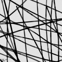
Note: Classical application methods of nano-lithography on a spin substrate Due to the specific interactions between these polymers and the substrate , in certain conditions, two types of polymers tend to create an intertwined pattern, there is a local order between the two polymers And forms amplitudes such as nanowires with a period in the range of 50 nm.
This pattern would be very useful if the subsequent application of the classic nano-lithography, which tends to accumulate on top of the polymer after landing on the layer due to less penetration mobility. Thus, the thin structure follows the polymer scaffold, which expands smoothly along different microns. However, the formed nanowires reveal some unwanted features as a closer look . Significant unevenness is observed in the fabrication of nanowires, and the nanowires are cut at certain points and deviate from the straight shape, which They are all typically the source of the deteriorating physical properties of nanowires. In addition, long-distance ordering of fabricated nanowire arrays does not follow this strategy, which is essential in certain applications such as the semiconductor industry.
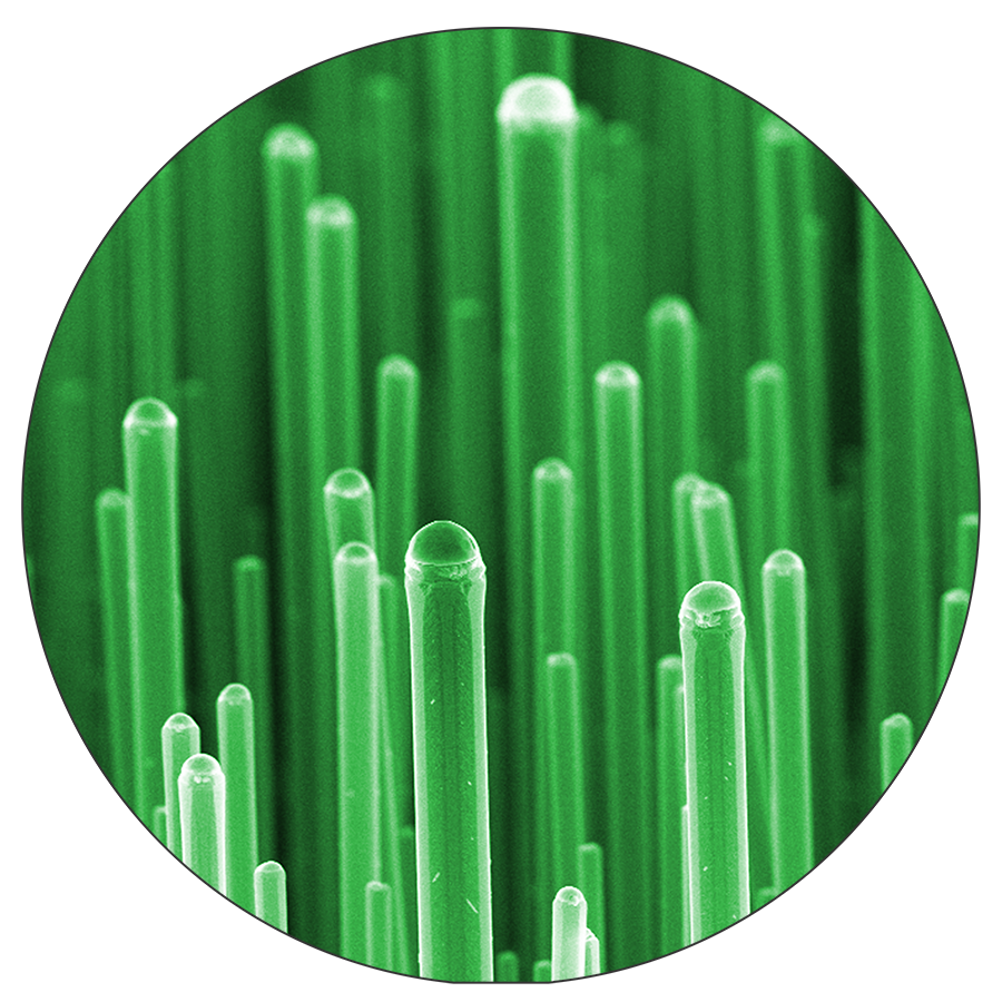
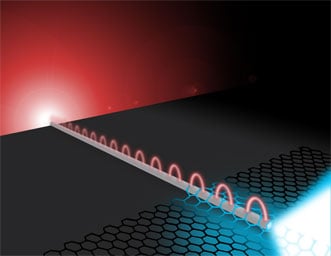
Nanowires are high-dimensional, large-area quasi-dielectric nanostructures in which radial strain uniformity allows unusable compounds of semiconductor materials. It enables countless applications of nanowires in electronics, optics and quantum technologies in general. In particle amplification, nanowires are synthesized by calculating the nanowire particles embedded in the alumina pattern in the air. The morphology and stages of nanowires / nanotubes are examined by transmission electron microscopy (TEM) and X-ray diffraction (XRD), respectively. Electron reaction of nanowire particles between oxidation is involved in the formation of such Nanowire nanostructures. This tiny nanowire is made up of nanoparticles with a diameter of nanometers Nanotechnology is the material in the approximate dimensions of 1 to 100 nanometers, where only one of its kind phenomena offers descriptive applications. Nanotechnology encompasses science, engineering, and non-scale technology, imaging, measuring, designing, and manipulating materials at this length scale. Due to nanotechnology, the speed of computers has increased and the value of computing has decreased. Nanowires are made on a flat surface of semiconductor materials such as silicon and germanium. Nanowires are very fine wires. They are made of metals such as silver, gold or iron. The nanometer is measured as a spatial measurement of about 9-10 meters, which is mostly used in nanotechnology to build nanomachines. This tiny nanowire is made up of nanoparticles about the size of a nanometer.

Conclusion :
Classical application methods of nano-lithography on an aspen substrate Due to the specific interactions between these polymers and the substrate , under certain conditions, two types of polymers tend to form an intertwined pattern, there is a local order between the two polymers and the range Forms such as nanowires with a period in the range of 50 nanometers.
Researcher and author: Dr. ( Afshin Rashid)
PhD in Nano-Microelectronics