Propagation of carbon nanotubes by method (plasma electric discharge) based on nano- microelectronics PHD (educational-research doctorate)
Researcher and author PhD student : Afshin Rashid
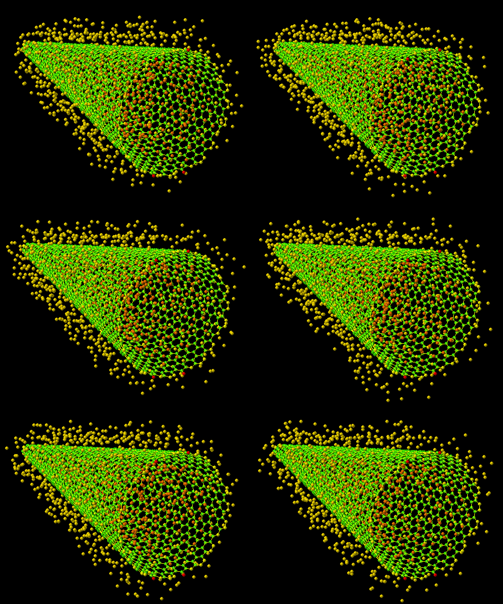
Note: This method of propagation of large currents passes through two carbon electrodes in a space containing plasma material, which leads to sparks in the gap between the two electrodes.
In this case, more than 30% of the ash produced is carbon nanotubes. A new method for the chemical modification of carbon nanotubes, which involves the radio frequency activation of the luminous plasma, followed by the chemical reactions characteristic of the plasma functional groups produced, is carbon nanotubes. For example, graphene chains on electron-guided carbon nanotubes react with plasma and are immobilized by the formation of base shelf bonds, which are stabilized by reduction with carbon nanotube particles. Using the same reaction, we also graft oxidized graphene chains with chemically dispersed pre-labeled bonds on carbon nanotubes under reaction with CNT carbon nanotubes. In this method, plasma multiplication of metal nanotubes and electron nanotubes Graphene labeling allows the surface's immobilization reaction to be performed simply by measuring light radiation. Single-layer (CNT) conductive carbon nanotubes are grafted.
There is a strong bond between the atoms of nanotubes, which makes them highly resistant to the effects of tensile forces . An example of the force required to break a carbon nanotube is many times the force required to break a piece of steel about the thickness of a nanotube. In nanotubes, inter-atomic bonds, in addition to creating high strength, make it easy to form and even twist . While steel is only resistant to tensile forces and does not have the necessary flexibility against twisting. Due to the good strength and ductility of nanotubes, they are used in composite materials with metal, polymer and ceramic fields as (filaments).
Conclusion:
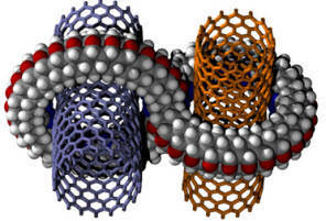
CNT carbon nanotubes have a similar structure to fullerene, the ends of which can be very thin. The name of these nanostructures is derived from their physical form, in which graphene-washed tubular sheets with different tubing angles lead to different symmetrical tubes . The angle of piping and the radius of the pipe determine the occurrence of metal or semiconductor properties in these nanostructures.
Author: PhD Student ( Afshin Rashid)


