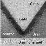
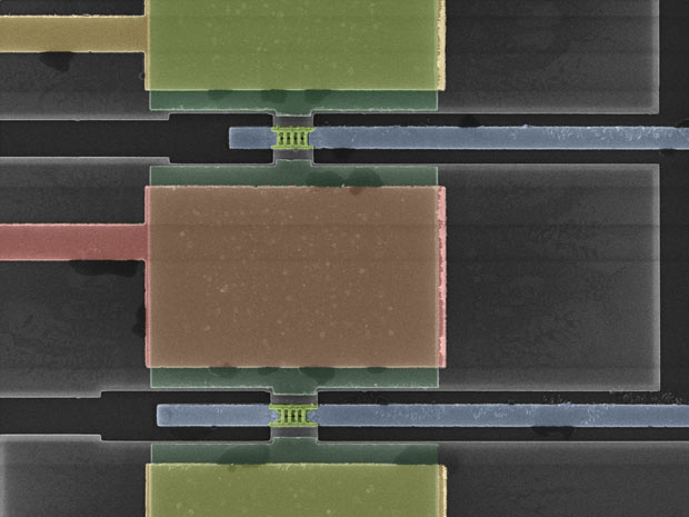
CMOS nanotransistors (PhD in nano-microelectronics)
Researcher and author: Dr. ( Afshin Rashid)
Note: Carbon nanotubes are tubes with graphene walls. These pipes can be single-walled or multi-walled. And is used in amplification of CMOS nanotransistors.
On the other hand, depending on how the carbon atoms are wrapped and arranged at the edge of the pipe, they can be found in three forms: chair handle, zigzag or 1. These three types of carbon nanotubes have very different properties. For example, two chiral chair handle structures behave like metal conductors, while the chiral structure behaves like a semiconductor, and its reaction with a small portion of the gap energy with carbon nanotubes has unique electrical and mechanical properties. For example, the structure of a nanotube, which is a thousand times larger than copper, and the metal nanotube is capable of carrying electric current at a density of cm / A, and these properties have led to its use in the manufacture of electronic devices such as CMOS (semiconductor) transistors. Be. Carbon nanotubes have been proposed as an alternative to silicon in the MOSFET transistor channel. Nanotubes can reduce some problems To greatly increase the channel length in the transistor, such as tunneling electrons from inside the channel or from the gate into the channel.
Nanotubes other than CMOS nanotransistors in the manufacture of meters and actuators ; Supercapacitors are also used in many other industries. The main problem with using nanotubes is mainly that they have to be used lying on the surface so that they can be bonded and metal bonded to achieve the CMOS transistor behavior. This is while the nanotubes grow vertically. In addition, it must be possible to precisely control the characteristics of each nanotube as well as its growth location and length. Increase the speed as much as possible to provide integrated electronics. Nanoelectronic circuits, especially RF blocks and microwaves, require very high-speed switches. Usually transistors with Record high speeds, up to 2 and heterogeneous bipolar MOSFET transistors and high electron mobility up to about 600GHz and 750GHz, respectively. These CMOS nanotransistors are combined with hybrid semiconductors, especially nanotubes . The main reason for the possibility of energy gap engineering in these compounds is unlike silicon.
Conclusion :
Carbon nanotubes are tubes with graphene walls. These pipes can be single-walled or multi-walled. And is used in amplification of CMOS nanotransistors.
Researcher and author: Dr. ( Afshin Rashid)
PhD in Nano-Microelectronics


