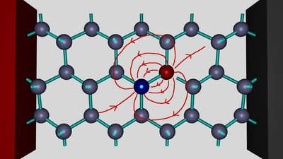
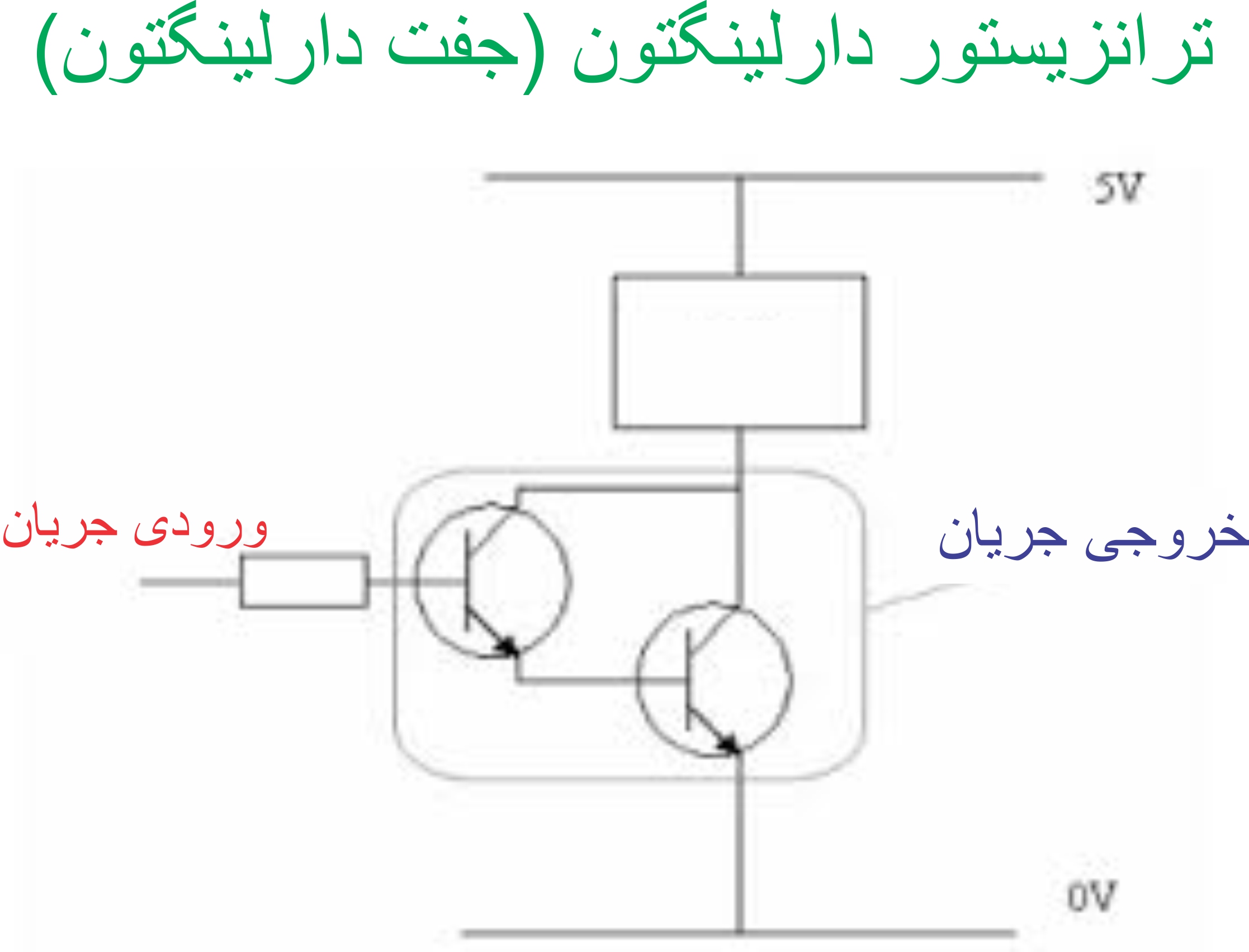
Section _ Understanding (Darlington transistor ) or Darlington pair
Examining ( Compound Supply) Bias Divider Voltage in Darlington Transistor = Pair or Even
Researcher and author: Dr. ( Afshin Rashid)
Note: However, in the self-powered method, the Rs resistor creates negative feedback to some extent, stabilizing the bias divider voltage of the Darlington transistor.
If we want the circuit to have the highest stability point, we use a circuit according to the bias divider voltage. In this circuit, the voltage divider bias R1 and R2 and the self-supply circuit (resistor RS) are used simultaneously. For this reason, this supply is also called a compound supply. Given that no current flows through the gate of the Darlington transistor pair, the emitter voltage is equal to the potential drop across the resistor R2, in other words, VDD is divided between R1 and R2 and VG is obtained from DD. Since this voltage is positive, in order for VGS to become negative, the collector potential, i.e. RSID, must be greater than VG so that the gate-emitter and collector junction arebias of the Darlington transistor pair .

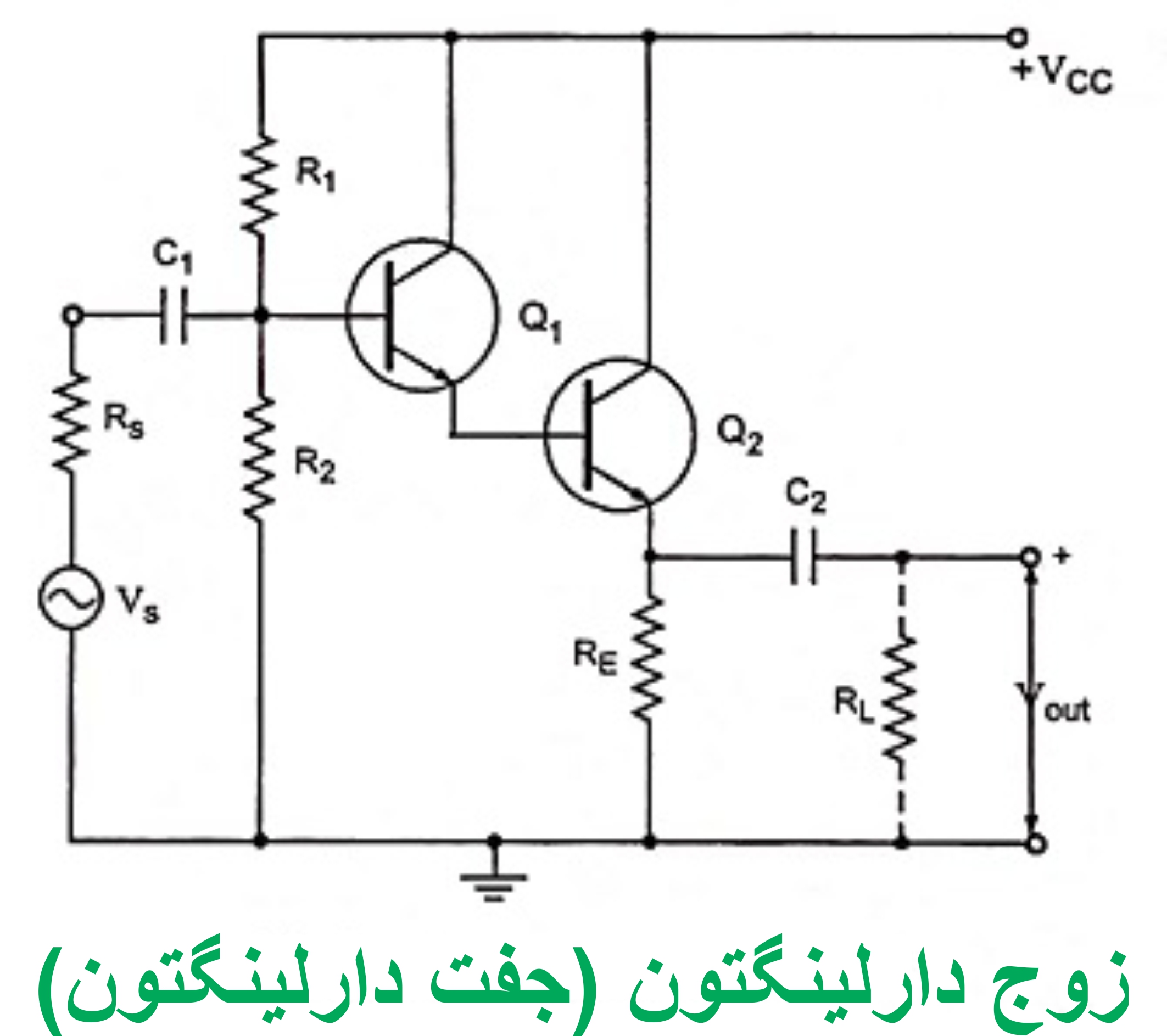
The resistive voltage in the Darlington transistor pair can also be obtained by using a transfer curve such as the bias plot analysis in the operating characteristic through the resistive voltage. In this plot, the load line on the VGS characteristic curve is not zero because the bias type resistors create a potential drop in the base or emitter at the voltage point. Therefore, in the divider of this circuit, the DC load line passes through the origin of the coordinates, that is, from a point in the DC voltage loop in the Darlington transistor pair or pair . The input to the circuit is not the DC voltage in the Darlington transistor pair or pair .